


 Material Insight: The Dielectric Constant of PCB Materials
 American Made Advocacy: What About the Rest of the Technology Stack?
 It’s Only Common Sense: Great Ideas From John Mitchell’s Book on Hiring Habits
A Quantum Leap
September 18, 2019 | University of California - Santa BarbaraEstimated reading time: 7 minutes
We hear a lot these days about the coming quantum revolution. Efforts to understand, develop, and characterize quantum materials — defined broadly as those displaying characteristics that can be explained only by quantum mechanics and not by classical physics — are intensifying.
Researchers around the world are racing to understand these materials and harness their unique qualities to develop revolutionary quantum technologies for quantum computing, communications, sensing, simulation and other quantum technologies not yet imaginable.
This week, UC Santa Barbara stepped to the front of that worldwide research race by being named the site of the nation’s first Quantum Foundry.
Funded by an initial six-year, $25-million grant from the National Science Foundation (NSF), the project, known officially as the UC Santa Barbara NSF Quantum Foundry, will involve 20 faculty members from the campus’s materials, physics, chemistry, mechanical engineering and computer science departments, plus myriad collaborating partners. The new center will be anchored within the California Nanosystems Institute (CNSI) in Elings Hall.
The grant provides substantial funding to build equipment and develop tools necessary to the effort. It also supports a multi-front research mission comprising collaborative interdisciplinary projects within a network of university, industry, and national-laboratory partners to create, process, and characterize materials for quantum information science. The Foundry will also develop outreach and educational programs aimed at familiarizing students at all levels with quantum science, creating a new paradigm for training students in the rapidly evolving field of quantum information science and engaging with industrial partners to accelerate development of the coming quantum workforce.
“We are extremely proud that the National Science Foundation has chosen UC Santa Barbara as home to the nation’s first NSF-funded Quantum Foundry,” said Chancellor Henry T. Yang. “The award is a testament to the strength of our University’s interdisciplinary science, particularly in materials, physics and chemistry, which lie at the core of quantum endeavors. It also recognizes our proven track record of working closely with industry to bring technologies to practical application, our state-of-the-art facilities and our educational and outreach programs that are mutually complementary with our research.
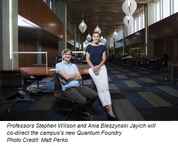
“Under the direction of physics professor Ania Bleszynski Jayich and materials professor Stephen Wilson the foundry will provide a collaborative environment for researchers to continue exploring quantum phenomena, designing quantum materials and building instruments and computers based on the basic principles of quantum mechanics,” Yang added.
Said Joseph Incandela, the campus’s vice chancellor for research, “UC Santa Barbara is a natural choice for the NSF quantum materials Foundry. We have outstanding faculty, researchers, and facilities, and a great tradition of multidisciplinary collaboration. Together with our excellent students and close industry partnerships, they have created a dynamic environment where research gets translated into important technologies.”
“Being selected to build and host the nation’s first Quantum Foundry is tremendously exciting and extremely important,” said Rod Alferness, dean of the College of Engineering. “It recognizes the vision and the decades of work that have made UC Santa Barbara a truly world-leading institution worthy of assuming a leadership role in a mission as important as advancing quantum science and the transformative technologies it promises to enable.”
“Advances in quantum science require a highly integrated interdisciplinary approach, because there are many hard challenges that need to be solved on many fronts,” said Bleszynski Jayich. “One of the big ideas behind the Foundry is to take these early theoretical ideas that are just beginning to be experimentally viable and use quantum mechanics to produce technologies that can outperform classical technologies.”
Doing so, however, will require new materials.
“Quantum technologies are fundamentally materials-limited, and there needs to be some sort of leap or evolution of the types of materials we can harness,” noted Wilson. “The Foundry is where we will try to identify and create those materials.”
Research Areas and Infrastructure
Quantum Foundry research will be pursued in three main areas, or “thrusts”:
- Natively Entangled Materials, which relates to identifying and characterizing materials that intrinsically host anyon excitations and long-range entangled states with topological, or structural, protection against decoherence. These include new intrinsic topological superconductors and quantum spin liquids, as well as materials that enable topological quantum computing.
- Interfaced Topological States, in which researchers will seek to create and control protected quantum states in hybrid materials.
- Coherent Quantum Interfaces, where the focus will be on engineering materials having localized quantum states that can be interfaced with various other quantum degrees of freedom (e.g. photons or phonons) for distributing quantum information while retaining robust coherence.
Developing these new materials and assessing their potential for hosting the needed coherent quantum state requires specialized equipment, much of which does not exist yet. A significant portion of the NSF grant is designated to develop such infrastructure, both to purchase required tools and equipment and to fabricate new tools necessary both to grow and characterize the quantum states in the new materials, Wilson said.
UC Santa Barbara’s deep well of shared materials growth and characterization infrastructure was also a factor in securing the grant. The Foundry will leverage existing facilities, such as the large suite of instrumentation shared via the Materials Research Lab and the California Nanosystems Institute, multiple molecular beam epitaxy (MBE) growth chambers (the university has the largest number of MBE apparatuses in academia), unique optical facilities such as the Terahertz Facility, state-of-the-art clean rooms, and others among the more than 300 shared instruments on campus.
Page 1 of 2
Share on:


Suggested Items
Material Insight: The Dielectric Constant of PCB Materials
05/17/2024 | Dr. Preeya Kuray -- Column: Material InsightIn the world of PCB design, miniaturization can be achieved by using low dielectric constant (Dk) materials. Low Dk materials can allow for a reduction in thickness while maintaining a given trace width, leading to lower transmission loss and higher density circuitry.
IPC APEX EXPO: Some Thoughts About Growth
05/16/2024 | Dan Feinberg, I-Connect007After two and a half days of wandering the aisles at IPC APEX EXPO 2024, for the first time, I almost felt like I was exploring CES. There were so many booths and exhibits that I could describe, but I’d like to focus on the growth and huge value of this event, which has expanded well beyond just the growing and impressive exhibit show floor.
The Shaughnessy Report: Unlock Your High-speed Material Constraints
05/15/2024 | Andy Shaughnessy -- Column: The Shaughnessy ReportThe world of PCB materials used to be a fairly simple one. It was divided into two groups: the “traditional” laminates, often called FR-4, and the high-speed laminates developed especially for high-speed PCBs. These were two worlds that usually didn’t collide. But then traditional laminates started getting better, and high-speed designers and design engineers took notice and started to reconsider what FR-4 could be used for.
Breaking High-speed Material Constraints: Design007 Magazine — May 2024
05/14/2024 | I-Connect007 Editorial TeamDo you need specialty materials for your high-speed designs? Maybe not. Improvements in resins mean designers of high-speed boards can sometimes use traditional laminate systems instead of high-speed materials, saving time and money while streamlining the fab process. In the May 2024 issue of Design007 Magazine, our contributors explain how to avoid overconstraining your materials when working with high-speed boards.
Indium Experts to Present at Electronics in Harsh Environments SMTA Conference
05/13/2024 | Indium Corporationndium Corporation Technical Manager for Europe, Africa, and the Middle East, Karthik Vijay, will deliver a technical presentation and Indium Corporation Senior Technologist, Dr. Ronald Lasky, will deliver both a workshop and technical presentation at the Electronics in Harsh Environments SMTA Conference on May 14-16 in Copenhagen, Denmark.