


 The Right Approach: I Hear the Train A Comin'
 It’s Only Common Sense: OCCAM—the Time Is Now
 Marcy's Musings: The Growing Industry
Intel Breaks Ground in the Silicon Heartland
September 12, 2022 | Business WireEstimated reading time: 2 minutes
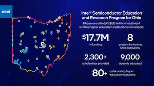
President Joe Biden joins Intel, Ohio Gov. Mike DeWine and other federal, state and local officials to celebrate breaking ground in the Silicon Heartland on two of the world's most advanced chipmaking facilities. As part of Intel’s commitment to develop a skilled talent pipeline for its two new leading-edge chip fabs, Intel also announced the first phase of funding for its Ohio Semiconductor Education and Research Program. During this first phase, Intel is providing $17.7 million for eight proposals from leading institutions and collaborators in Ohio to develop semiconductor-focused education and workforce programs.
“Today marks a pivotal moment in the journey to build a more geographically balanced and resilient semiconductor supply chain. The establishment of the Silicon Heartland is testament to the power of government incentives to unlock private investment, create thousands of high-paying jobs, and benefit U.S. economic and national security. We would not be here today without the support of leaders in the administration, Congress and the state of Ohio, who share a vision to help restore the United States to its rightful place as a leader in advanced chipmaking,” said Pat Gelsinger, Intel CEO.
Semiconductors are the brains behind the technology that powers our digital age. These chips are critical to the foundations of the U.S. economy, national security and technology leadership. Investing to revitalize the U.S. chipmaking ecosystem will bring a broad range of economic benefits, while helping to restore balance, dependability and resilience to the global semiconductor supply chain.
In Ohio, Intel’s more than $20 billion planned investment in a new semiconductor manufacturing site to produce leading-edge chips is expected to generate 7,000 construction jobs and 3,000 long-term positions in manufacturing and engineering. In addition to providing capacity for Intel’s next-generation products, the company expects these new factories to support growing demand for the company’s new foundry business, Intel Foundry Services (IFS).
How Intel Supports U.S. Research and Development (R&D) and Manufacturing: Intel’s investment in Ohio builds on the company’s announcement in Arizona to build two new fabs and its expansion in New Mexico to add advanced packaging capabilities. When combined with Intel’s silicon R&D capabilities, this new site in Licking County, Ohio, will expand the company’s U.S. “lab-to-fab” pipeline.
Intel also recently celebrated the grand opening of the latest expansion of its leading-edge developmental factory in Oregon, where engineers advance Moore’s Law by creating new transistor architectures, wafer processes and packaging technologies that underpin the company’s product roadmap. That investment represents the next phase of Intel’s commitment to driving U.S. leadership in semiconductor research and development.
Share on:


Suggested Items
Real Time with… IPC APEX EXPO 2024: Tools, Training, and Trends in Manufacturing Engineering
04/25/2024 | Real Time with...IPC APEX EXPOGuest Editor Kelly Dack and Product Specialist Erik Bateham of Polar Instruments discuss Polar's latest technology, including their role in aiding manufacturing engineers. They highlight the advanced capabilities of Polar's tools and the critical role of signal integrity analysis, as well as the importance of accurate modeling in board manufacturing. Polar's unique training approach and demonstration contact details are also explored.
TTM Celebrates the Grand Opening of Its First Manufacturing Facility in Penang
04/25/2024 | TTM Technologies, Inc.TTM Technologies, Inc., a leading global manufacturer of technology solutions including mission systems, radio frequency (RF) components and RF microwave/microelectronic assemblies, and quick-turn and technologically advanced printed circuit boards (PCBs), officially opened its first manufacturing plant in Penang, Malaysia with an investment of USD200 million (approximately RM958 million).
Listen Up! The Intricacies of PCB Drilling Detailed in New Podcast Episode
04/25/2024 | I-Connect007In episode 5 of the podcast series, On the Line With: Designing for Reality, Nolan Johnson and Matt Stevenson continue down the manufacturing process, this time focusing on the post-lamination drilling process for PCBs. Matt and Nolan delve into the intricacies of the PCB drilling process, highlighting the importance of hole quality, drill parameters, and design optimization to ensure smooth manufacturing. The conversation covers topics such as drill bit sizes, aspect ratios, vias, challenges in drilling, and ways to enhance efficiency in the drilling department.
Elevating PCB Design Engineering With IPC Programs
04/24/2024 | Cory Blaylock, IPCIn a monumental stride for the electronics manufacturing industry, IPC has successfully championed the recognition of the PCB Design Engineer as an official occupation by the U.S. Department of Labor (DOL). This pivotal achievement not only underscores the critical role of PCB design engineers within the technology landscape, but also marks the beginning of a transformative journey toward nurturing a robust, skilled workforce ready to propel our industry into the future.
Fujitsu, METRON Collaborate to Drive ESG Success
04/24/2024 | JCN NewswireFujitsu Limited and METRON SAS, a French cleantech company specializing in energy management solutions for industrial decarbonization, today announced a strategic initiative to contribute to the realization of carbon neutrality in the manufacturing industry.