


 The Right Approach: I Hear the Train A Comin'
 It’s Only Common Sense: OCCAM—the Time Is Now
 Marcy's Musings: The Growing Industry
Nikon Announces Investment in Hybrid Manufacturing Technologies Global
September 16, 2022 | NikonEstimated reading time: 2 minutes
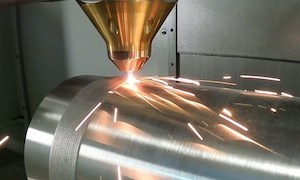
Nikon Corporation announced an investment in Hybrid Manufacturing Technologies Global, Inc. Hybrid Manufacturing Technologies Global, Inc. (HMT), an award-winning industry leader in additive manufacturing (AM), successfully created an approach that enables users to integrate additive tools onto any platform. This groundbreaking technology allows users to take full advantage of the manufacturing process by unifying multiple complementary technologies in one set up.
Parts manufacturers will often use AM processing and machining in tandem, depending upon their specific production goals and tolerances. HMT enabled a game-changing leap forward by unlocking the freedoms of additive while retaining the precision and surface finish capabilities of CNC, all in a single system. When using their patented AMBIT™ deposition heads only a simple tool change is required to switch from cutting to adding metal, giving users unprecedented flexibility. HMT's tool changeable heads are not limited to laser processes but are also compatible with numerous materials and a vast array of deployment methods. HMT can upgrade existing vertical platforms to enable both additive and subtractive machining capabilities in one system or create bespoke solutions with customized heads to meet the user's objectives.
Nikon manufactures some of the most precise equipment in the world, with its products being used in applications ranging from semiconductor manufacturing and mass production of panels for televisions and smart devices, to medical systems, automotive and satellites. Nikon established the Next Generation Project Division to accelerate the launch of new growth businesses, including advanced materials processing technologies, through synergies resulting from strategic investments and alliances with industry-leading companies worldwide.
This latest investment will enable HMT and Nikon to leverage their combined expertise to accelerate innovation and expand the hybrid manufacturing landscape. Yuichi Shibazaki, Nikon Corporate Vice President and General Manager of the Next Generation Project Division said, "This investment in HMT is the latest component of our Next Generation Project program to further industrialization of digital manufacturing. As an industry leader with demonstrated collaborative capabilities, HMT and its AMBIT™ portfolio are well-matched with Nikon technologies. We look forward to working with them as part of our commitment to creating value and advancing society through novel industries like hybrid manufacturing."
Dr. Jason B. Jones, HMT Co-founder and CEO, said, "We are honored to receive investment from such a longstanding technology leader as Nikon. Together we will more fully deliver on the promise of additive and digital manufacturing. We expect the results of this technology will touch the lives of virtually all people on earth in the coming decades."
"Hybrid is all about synergy," Peter Coates, HMT Co-founder and CTO added. "For the better part of ten years in this industry we have taken pride in the strategic nature of our collaborations and our partnership with Nikon takes this to a whole new level by adding value to advanced manufacture."
Share on:


Suggested Items
Real Time with… IPC APEX EXPO 2024: Tools, Training, and Trends in Manufacturing Engineering
04/25/2024 | Real Time with...IPC APEX EXPOGuest Editor Kelly Dack and Product Specialist Erik Bateham of Polar Instruments discuss Polar's latest technology, including their role in aiding manufacturing engineers. They highlight the advanced capabilities of Polar's tools and the critical role of signal integrity analysis, as well as the importance of accurate modeling in board manufacturing. Polar's unique training approach and demonstration contact details are also explored.
TTM Celebrates the Grand Opening of Its First Manufacturing Facility in Penang
04/25/2024 | TTM Technologies, Inc.TTM Technologies, Inc., a leading global manufacturer of technology solutions including mission systems, radio frequency (RF) components and RF microwave/microelectronic assemblies, and quick-turn and technologically advanced printed circuit boards (PCBs), officially opened its first manufacturing plant in Penang, Malaysia with an investment of USD200 million (approximately RM958 million).
Listen Up! The Intricacies of PCB Drilling Detailed in New Podcast Episode
04/25/2024 | I-Connect007In episode 5 of the podcast series, On the Line With: Designing for Reality, Nolan Johnson and Matt Stevenson continue down the manufacturing process, this time focusing on the post-lamination drilling process for PCBs. Matt and Nolan delve into the intricacies of the PCB drilling process, highlighting the importance of hole quality, drill parameters, and design optimization to ensure smooth manufacturing. The conversation covers topics such as drill bit sizes, aspect ratios, vias, challenges in drilling, and ways to enhance efficiency in the drilling department.
Elevating PCB Design Engineering With IPC Programs
04/24/2024 | Cory Blaylock, IPCIn a monumental stride for the electronics manufacturing industry, IPC has successfully championed the recognition of the PCB Design Engineer as an official occupation by the U.S. Department of Labor (DOL). This pivotal achievement not only underscores the critical role of PCB design engineers within the technology landscape, but also marks the beginning of a transformative journey toward nurturing a robust, skilled workforce ready to propel our industry into the future.
Fujitsu, METRON Collaborate to Drive ESG Success
04/24/2024 | JCN NewswireFujitsu Limited and METRON SAS, a French cleantech company specializing in energy management solutions for industrial decarbonization, today announced a strategic initiative to contribute to the realization of carbon neutrality in the manufacturing industry.