


 The Right Approach: I Hear the Train A Comin'
 It’s Only Common Sense: OCCAM—the Time Is Now
 Marcy's Musings: The Growing Industry
NEC Develops First Highly Sensitive Uncooled Infrared Image Sensor Utilizing Carbon Nanotubes
April 10, 2023 | JCN NewswireEstimated reading time: 2 minutes
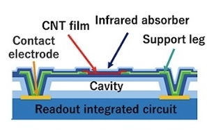
NEC Corporation has succeeded in developing the world's first high-sensitivity uncooled infrared image sensor that uses high-purity semiconducting carbon nanotubes (CNTs) in the infrared detection area. This was accomplished using NEC's proprietary extraction technology. NEC will work toward the practical application of this image sensor in 2025.
Infrared image sensors convert infrared rays into electrical signals to acquire necessary information, and can detect infrared rays emitted from people and objects even in the dark. Therefore, infrared image sensors are utilized in various fields to provide a safe and secure social infrastructure, such as night vision to support automobiles driving in the darkness, aircraft navigation support systems and security cameras.
There are two types of infrared image sensors, the "cooled type," which operates at extremely low temperatures, and the "uncooled type," which operates near room temperature. The cooled type is highly sensitive and responsive, but requires a cooler, which is large, expensive, consumes a great deal of electricity, and requires regular maintenance. On the other hand, the uncooled type does not require a cooler, enabling it to be compact, inexpensive, and to consume low power, but it has the issues of inferior sensitivity and resolution compared to the cooled type.
In 1991, NEC discovered CNTs for the first time in the world and is now a leader in research and development related to nanotechnology. In 2018, NEC developed a proprietary technology to extract only semiconducting-type CNTs at high purity from single-walled CNTs that have a mixture of metallic and semiconducting types. NEC then discovered that thin films of semiconducting-type CNTs extracted with this technology have a large temperature coefficient of resistance (TCR) near room temperature.
The newly developed infrared image sensor is the result of these achievements and know-how. NEC applied semiconductor-type CNTs based on its proprietary technology that features a high TCR, which is an important index for high sensitivity. As a result, the new sensor achieves more than three times higher sensitivity than mainstream uncooled infrared image sensors using vanadium oxide or amorphous silicon.
The new device structure was achieved by combining the thermal separation structure used in uncooled infrared image sensors, the Micro Electro Mechanical Systems (MEMS) device technology used to realize this structure, and the CNT printing and manufacturing technology cultivated over many years for printed transistors, etc. As a result, NEC has succeeded in operating a high-definition uncooled infrared image sensor of 640 x 480 pixels by arraying the components of the structure.
Part of this work was done in collaboration with Japan's National Institute of Advanced Industrial Science and Technology (AIST). In addition, a part of this achievement was supported by JPJ004596, a security technology research promotion program conducted by Japan's Acquisition, Technology & Logistics Agency (ATLA).
Going forward, NEC will continue its research and development to further advance infrared image sensor technologies and to realize products and services that can contribute to various fields and areas of society.
Share on:


Suggested Items
Warm Windows and Streamlined Skin Patches – IDTechEx Explores Flexible and Printed Electronics
04/26/2024 | IDTechExFlexible and printed electronics can be integrated into cars and homes to create modern aesthetics that are beneficial and easy to use. From luminous car controls to food labels that communicate the quality of food, the uses of this technology are endless and can upgrade many areas of everyday life.
iNEMI Packaging Tech Topic Series: Role of EDA in Advanced Semiconductor Packaging
04/26/2024 | iNEMIAdvanced semiconductor packaging with heterogenous integration has made on-package integration of multiple chips a crucial part of finding alternatives to transistor scaling. Historically, EDA tools for front-end and back-end design have evolved separately; however, design complexity and the increased number of die-to-die or die-to-substrate interconnections has led to the need for EDA tools that can support integration of overall design planning, implementation, and system analysis in a single cockpit.
Koh Young Showcases Award-winning Inspection Solutions at SMTconnect with SmartRep in Hall 4A.225
04/25/2024 | Koh Young TechnologyKoh Young Technology, the industry leader in True 3D measurement-based inspection solutions, will showcase an array of award-winning inspection and measurement solutions at SMTconnect alongside its sales partner, SmartRep, in booth 4A.225 at NürnbergMesse from June 11-13, 2023. The following offers a glimpse into what Koh Young will present at the tradeshow:
Real Time with… IPC APEX EXPO 2024: Plasmatreat: Innovative Surface Preparation Solutions
04/25/2024 | Real Time with...IPC APEX EXPOIn this interview, Editor Nolan Johnson speaks with Hardev Grewal, CEO and president of Plasmatreat, a developer of atmospheric plasma solutions. Plasmatreat uses clean compressed air and electricity to create plasma, offering environmentally friendly methods for surface preparation. Their technology measures plasma density for process optimization and can remove organic micro-contamination. Nolan and Hardev also discuss REDOX-Tool, a new technology for removing metal oxides.
Nanotechnology Market to Surpass $53.51 Billion by 2031
04/25/2024 | PRNewswireSkyQuest projects that the nanotechnology market will attain a value of USD 53.51 billion by 2031, with a CAGR of 36.4% over the forecast period (2024-2031).