


 The Right Approach: I Hear the Train A Comin'
 It’s Only Common Sense: OCCAM—the Time Is Now
 Marcy's Musings: The Growing Industry
Ansys Joins TSMC's OIP Cloud Alliance for Secure Multiphysics Analysis in the Cloud
April 27, 2023 | ANSYSEstimated reading time: 1 minute
Ansys announced that it has joined TSMC's OIP Cloud Alliance to facilitate the deployment of fully distributed workflows for mutual customers. By driving toward the cloud interoperability of Ansys multiphysics solutions with TSMC's technology enablement, customers will easily be able to gain the full benefits of faster run times and elastic computing with major cloud vendors.
Combining EDA parallelism and cloud scalability, TSMC and its OIP Cloud Alliance partners are creating next-generation, cloud-optimized design methodologies to further accelerate turnaround time of critical design tasks. Ansys and other EDA partners will optimize their tools for multi-threaded, fully-distributed runs to best utilize cloud, while cloud partners will bring new virtual machines most suitable for the EDA workload of IC designs.
"Our customers of all sizes are leveraging the cloud to boost productivity while designing in TSMC's leading-edge technologies for new applications from high performance computing to mobile, artificial intelligence, networking, and 3D-IC," said Dan Kochpatcharin, head of the Design Infrastructure Management Division at TSMC. "By welcoming Ansys as the latest member into our OIP Cloud Alliance, TSMC aims to make Ansys' leading multiphysics signoff solutions available to all of our customers and help them bring their differentiated products to market sooner, with higher quality."
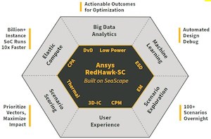
Ansys was an early adopter of elastic cloud computing with its SeaScape big-data platform – a cloud-native data infrastructure that was designed specifically for EDA. Ansys® RedHawk-SC™ was the first tool built to work with SeaScape (SC) and many other Ansys semiconductor tools have followed, including Ansys® PathFinder-SC™, Ansys® Totem-SC™, and Ansys® PowerArtist-SC™.
"Ansys' strategy for the future foresees an absolutely central role for cloud computing," said John Lee, vice president and general manager of the semiconductor, electronics, and optics business unit at Ansys. "We have invested heavily in cloud-enabled platforms that give our products clear advantages in speed and capacity over traditional tool environments that were not designed for the cloud."
Share on:


Suggested Items
iNEMI Packaging Tech Topic Series: Role of EDA in Advanced Semiconductor Packaging
04/26/2024 | iNEMIAdvanced semiconductor packaging with heterogenous integration has made on-package integration of multiple chips a crucial part of finding alternatives to transistor scaling. Historically, EDA tools for front-end and back-end design have evolved separately; however, design complexity and the increased number of die-to-die or die-to-substrate interconnections has led to the need for EDA tools that can support integration of overall design planning, implementation, and system analysis in a single cockpit.
Cadence, TSMC Collaborate on Wide-Ranging Innovations to Transform System and Semiconductor Design
04/25/2024 | Cadence Design SystemsCadence Design Systems, Inc. and TSMC have extended their longstanding collaboration by announcing a broad range of innovative technology advancements to accelerate design, including developments ranging from 3D-IC and advanced process nodes to design IP and photonics.
Ansys, TSMC Enable a Multiphysics Platform for Optics and Photonics, Addressing Needs of AI, HPC Silicon Systems
04/25/2024 | PRNewswireAnsys announced a collaboration with TSMC on multiphysics software for TSMC's Compact Universal Photonic Engines (COUPE). COUPE is a cutting-edge Silicon Photonics (SiPh) integration system and Co-Packaged Optics platform that mitigates coupling loss while significantly accelerating chip-to-chip and machine-to-machine communication.
Siemens’ Breakthrough Veloce CS Transforms Emulation and Prototyping with Three Novel Products
04/24/2024 | Siemens Digital Industries SoftwareSiemens Digital Industries Software launched the Veloce™ CS hardware-assisted verification and validation system. In a first for the EDA (Electronic Design Automation) industry, Veloce CS incorporates hardware emulation, enterprise prototyping and software prototyping and is built on two highly advanced integrated circuits (ICs) – Siemens’ new, purpose-built Crystal accelerator chip for emulation and the AMD Versal™ Premium VP1902 FPGA adaptive SoC (System-on-a-chip) for enterprise and software prototyping.
Listen Up! The Intricacies of PCB Drilling Detailed in New Podcast Episode
04/25/2024 | I-Connect007In episode 5 of the podcast series, On the Line With: Designing for Reality, Nolan Johnson and Matt Stevenson continue down the manufacturing process, this time focusing on the post-lamination drilling process for PCBs. Matt and Nolan delve into the intricacies of the PCB drilling process, highlighting the importance of hole quality, drill parameters, and design optimization to ensure smooth manufacturing. The conversation covers topics such as drill bit sizes, aspect ratios, vias, challenges in drilling, and ways to enhance efficiency in the drilling department.