


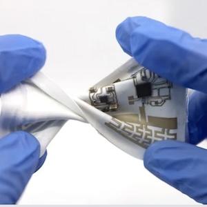


 Flexible Thinking: PCB Designers Still Wanted
 Connect the Dots: Five Best Practices for Designing Flex and Rigid-flex PCBs
 Tim’s Takeaways: Human Ingenuity and the Rigid-flex PCB
Ansys Joins TSMC's OIP Cloud Alliance for Secure Multiphysics Analysis in the Cloud
April 27, 2023 | ANSYSEstimated reading time: 1 minute
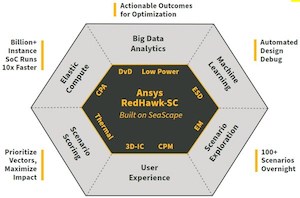
Ansys announced that it has joined TSMC's OIP Cloud Alliance to facilitate the deployment of fully distributed workflows for mutual customers. By driving toward the cloud interoperability of Ansys multiphysics solutions with TSMC's technology enablement, customers will easily be able to gain the full benefits of faster run times and elastic computing with major cloud vendors.
Combining EDA parallelism and cloud scalability, TSMC and its OIP Cloud Alliance partners are creating next-generation, cloud-optimized design methodologies to further accelerate turnaround time of critical design tasks. Ansys and other EDA partners will optimize their tools for multi-threaded, fully-distributed runs to best utilize cloud, while cloud partners will bring new virtual machines most suitable for the EDA workload of IC designs.
"Our customers of all sizes are leveraging the cloud to boost productivity while designing in TSMC's leading-edge technologies for new applications from high performance computing to mobile, artificial intelligence, networking, and 3D-IC," said Dan Kochpatcharin, head of the Design Infrastructure Management Division at TSMC. "By welcoming Ansys as the latest member into our OIP Cloud Alliance, TSMC aims to make Ansys' leading multiphysics signoff solutions available to all of our customers and help them bring their differentiated products to market sooner, with higher quality."
Ansys was an early adopter of elastic cloud computing with its SeaScape big-data platform – a cloud-native data infrastructure that was designed specifically for EDA. Ansys® RedHawk-SC™ was the first tool built to work with SeaScape (SC) and many other Ansys semiconductor tools have followed, including Ansys® PathFinder-SC™, Ansys® Totem-SC™, and Ansys® PowerArtist-SC™.
"Ansys' strategy for the future foresees an absolutely central role for cloud computing," said John Lee, vice president and general manager of the semiconductor, electronics, and optics business unit at Ansys. "We have invested heavily in cloud-enabled platforms that give our products clear advantages in speed and capacity over traditional tool environments that were not designed for the cloud."
Share on:


Suggested Items
I-Connect007 Editor’s Choice: Five Must-Reads for the Week
05/31/2024 | Marcy LaRont, PCB007 MagazineThis week, our columnists enjoy particular attention with Barry Olney, Mehul Dave, and Happy Holden all providing valuable insight on materials, the critical importance of the front-end engineering process once a PCB design is received, and an overview and observations around IPC APEX EXPO technical sessions.
Bell Awarded Funding for Phase 1B of DARPA Speed and Runway Independent Technologies (SPRINT) X-Plane Program
05/30/2024 | BellBell Textron Inc., a Textron Inc. company, has been down-selected for Phase 1B of Defense Advanced Research Projects Agency (DARPA) Speed and Runway Independent Technologies (SPRINT) X-Plane program.
Cambridge GaN Devices Signs MoU with ITRI Covering GaN-based Power Supply Development
05/30/2024 | BUSINESS WIRECambridge GaN Devices (CGD), the fabless, clean-tech semiconductor company, dedicating to develop energy-efficient GaN-based power devices that make greener electronics possible, has signed a Memorandum of Understanding with Industrial Technology Research Institute (ITRI) of Taiwan to solidify a partnership in developing high performance GaN solutions for USB-PD adaptors.
Connect the Dots: Designing for Reality—The Physical Manufacturing Phases
05/30/2024 | Matt Stevenson -- Column: Connect the DotsDesigning for reality is focused on the art and science of PCB design and production. If you’re trying to make a PCB that stands out for being reliable, easy to manufacture, and meets all design goals, then you’re in the perfect spot. We’re here to break down the PCB manufacturing process while sharing essential tips for smooth design and production.
Elementary, Mr. Watson: Pushing Design Boundaries
05/29/2024 | John Watson -- Column: Elementary, Mr. WatsonOverconstraint: What a concept. Our first thoughts would be: What are we hurting by overconstraining a design? Isn't it better to be safe than sorry? What is meant by overconstraint? It means to apply excessive constraints. In engineering and mathematics, it's used when there are too many simultaneous equations to result in an exact solution. For example, fitting a line to many points is overconstrained because a line cannot be drawn simultaneously through all of the points. In PCB design, overconstraints always occur, including dimensional, electrical, manufacturing, and timing constraints. The list goes on.