


 The Right Approach: I Hear the Train A Comin'
 It’s Only Common Sense: OCCAM—the Time Is Now
 Marcy's Musings: The Growing Industry
Analog Devices Further Strengthens its South-East Asia Operations with New Singapore Facility
May 31, 2023 | ACN NewswireEstimated reading time: 2 minutes
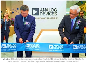
Analog Devices, Inc., a global semiconductor leader, announced the launch of a new state-of-the-art, environmentally friendly, 38,951 sq. ft. facility in Singapore. Located within the Kallang Industrial Park, the facility is planned to serve as a central hub for the more than 200 employees working in Singapore in key divisions of the company, including research and development, test engineering, sales, and manufacturing. ADI established its first location in Singapore in 1995 and has steadily grown its operations and workforce since then. This new strategic investment aligns with the company's global expansion plans, which include enhancing its capabilities in the Asia Pacific region.
"Our new facility is an important milestone in ADI's global growth strategy," said Jerry Fan, President of Asia for ADI. "Enhancing our capabilities in Singapore is vital to leveraging the country's superb talent pool and advanced manufacturing capabilities to serve our regional and global customers' needs. Our investment reinforces ADI's presence within Singapore's thriving semiconductor ecosystem, which is supported by the nation's digital growth initiatives."
The new facility features a more spacious and advanced laboratory to foster interaction between the research and development team as well as customers in the region. Through this forum for the exchange of ideas, ADI and its customers plan to deepen their collaboration and deliver innovative products for the Intelligent Edge. In addition, a dedicated space has been allocated for test development purposes within the new facility, custom-tailored to accommodate multiple automated test equipment (ATE) stations. These on-site testing stations are designed to enable faster initial testing of ADI's state-of-the-art products and accelerate the timeline of ADI engineering's ability to meet customers' toughest challenges.
Fan continued, "Customer intimacy, business strategy, engineering processes, manufacturing capabilities, and problem-solving are essential for creating long-term value for our customers. We are confident the environment within our new facility will help us deliver the kind of innovation that leads to breakthrough products and services, and we believe it will have a lasting impact on the region's ongoing digital transformation journey."
Location selection and build criteria for the site prioritized accessibility and sustainability. The new office is bicycle-friendly, close to public transportation, and is directly accessible via expressways. Recyclable materials were used throughout construction, and energy efficient AC, lighting, and water systems are all part of its advanced building automation system. Low carbon footprint materials were an integral part of the biophilic interior design. The office building is Green Mark Platinum-certified and expected to get LEED Gold certification by July 2023.
Share on:


Suggested Items
Real Time with… IPC APEX EXPO 2024: Tools, Training, and Trends in Manufacturing Engineering
04/25/2024 | Real Time with...IPC APEX EXPOGuest Editor Kelly Dack and Product Specialist Erik Bateham of Polar Instruments discuss Polar's latest technology, including their role in aiding manufacturing engineers. They highlight the advanced capabilities of Polar's tools and the critical role of signal integrity analysis, as well as the importance of accurate modeling in board manufacturing. Polar's unique training approach and demonstration contact details are also explored.
TTM Celebrates the Grand Opening of Its First Manufacturing Facility in Penang
04/25/2024 | TTM Technologies, Inc.TTM Technologies, Inc., a leading global manufacturer of technology solutions including mission systems, radio frequency (RF) components and RF microwave/microelectronic assemblies, and quick-turn and technologically advanced printed circuit boards (PCBs), officially opened its first manufacturing plant in Penang, Malaysia with an investment of USD200 million (approximately RM958 million).
Listen Up! The Intricacies of PCB Drilling Detailed in New Podcast Episode
04/25/2024 | I-Connect007In episode 5 of the podcast series, On the Line With: Designing for Reality, Nolan Johnson and Matt Stevenson continue down the manufacturing process, this time focusing on the post-lamination drilling process for PCBs. Matt and Nolan delve into the intricacies of the PCB drilling process, highlighting the importance of hole quality, drill parameters, and design optimization to ensure smooth manufacturing. The conversation covers topics such as drill bit sizes, aspect ratios, vias, challenges in drilling, and ways to enhance efficiency in the drilling department.
Elevating PCB Design Engineering With IPC Programs
04/24/2024 | Cory Blaylock, IPCIn a monumental stride for the electronics manufacturing industry, IPC has successfully championed the recognition of the PCB Design Engineer as an official occupation by the U.S. Department of Labor (DOL). This pivotal achievement not only underscores the critical role of PCB design engineers within the technology landscape, but also marks the beginning of a transformative journey toward nurturing a robust, skilled workforce ready to propel our industry into the future.
Fujitsu, METRON Collaborate to Drive ESG Success
04/24/2024 | JCN NewswireFujitsu Limited and METRON SAS, a French cleantech company specializing in energy management solutions for industrial decarbonization, today announced a strategic initiative to contribute to the realization of carbon neutrality in the manufacturing industry.