


 The Right Approach: I Hear the Train A Comin'
 It’s Only Common Sense: OCCAM—the Time Is Now
 Marcy's Musings: The Growing Industry
3D Plasmon Antenna Capable of Focusing Light into Few Nanometers
June 26, 2015 | KAISTEstimated reading time: 1 minute
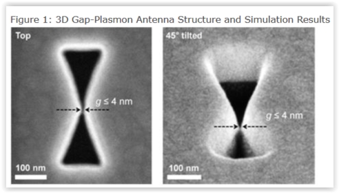
Professors Myung-Ki Kim and Yong-Hee Lee, both of the Physics Department at KAIST, and their research teams have developed a three dimensional (3D) gap-plasmon antenna which can focus light into a space a few nanometers wide. Their research findings were published in the June 10th issue of Nano Letters.
Focusing light into a point-like space is an active research field with many applications. However, concentrating light into a smaller space than its wavelength is often hindered by diffraction. To tackle this problem, many researchers have utilized the plasmonic phenomenon of a metal where light can be confined to a greater extent by overcoming the diffraction limit.
Many researchers have focused on developing a two dimensional (2D) plasmon antenna and were able to focus a light under 5 nanometers wide. However, this 2D antenna revealed a challenge: the light disperses to the opposite end regardless of how small its beam was focused. To solve this difficulty, a 3D structure had to be employed to maximize the light's intensity.
Adopting the proximal focused-ion-beam milling technology, the KAIST research team developed a 3D four nanometer wide gap-plasmon antenna. By squeezing the photons into a 3D nano space of 4 x 10 x 10 nm3 size, the researchers were able to increase the intensity of light by 400,000 times stronger than that of the incident light. Capitalizing on the enhanced intensity of light within the antenna, they intensified the second-harmonic signal and verified that the light was focused in the nano gap by scanning cathodoluminescent images.
The researchers anticipate that this technology will improve the speed of data transfer and processing up to the level of a terahertz (one trillion times per second) and to enlarge the storage volume per unit area on hard disks by 100 times. In addition, high definition images of submolecule size can be taken with actual light, instead of with an electron microscope, while improving the semiconductor process to a smaller size of few nanometers.
Professor Kim said, “A simple yet ingenious idea has shifted the research paradigm from 2D gap-plasmon antennas to 3D antennas. This technology will see numerous applications including in the field of information technology, data storage, imaging medical science, and semiconductor processes.”
The research was sponsored by the National Research Foundation of Korea.
Share on:


Suggested Items
Warm Windows and Streamlined Skin Patches – IDTechEx Explores Flexible and Printed Electronics
04/26/2024 | IDTechExFlexible and printed electronics can be integrated into cars and homes to create modern aesthetics that are beneficial and easy to use. From luminous car controls to food labels that communicate the quality of food, the uses of this technology are endless and can upgrade many areas of everyday life.
iNEMI Packaging Tech Topic Series: Role of EDA in Advanced Semiconductor Packaging
04/26/2024 | iNEMIAdvanced semiconductor packaging with heterogenous integration has made on-package integration of multiple chips a crucial part of finding alternatives to transistor scaling. Historically, EDA tools for front-end and back-end design have evolved separately; however, design complexity and the increased number of die-to-die or die-to-substrate interconnections has led to the need for EDA tools that can support integration of overall design planning, implementation, and system analysis in a single cockpit.
Koh Young Showcases Award-winning Inspection Solutions at SMTconnect with SmartRep in Hall 4A.225
04/25/2024 | Koh Young TechnologyKoh Young Technology, the industry leader in True 3D measurement-based inspection solutions, will showcase an array of award-winning inspection and measurement solutions at SMTconnect alongside its sales partner, SmartRep, in booth 4A.225 at NürnbergMesse from June 11-13, 2023. The following offers a glimpse into what Koh Young will present at the tradeshow:
Real Time with… IPC APEX EXPO 2024: Plasmatreat: Innovative Surface Preparation Solutions
04/25/2024 | Real Time with...IPC APEX EXPOIn this interview, Editor Nolan Johnson speaks with Hardev Grewal, CEO and president of Plasmatreat, a developer of atmospheric plasma solutions. Plasmatreat uses clean compressed air and electricity to create plasma, offering environmentally friendly methods for surface preparation. Their technology measures plasma density for process optimization and can remove organic micro-contamination. Nolan and Hardev also discuss REDOX-Tool, a new technology for removing metal oxides.
Nanotechnology Market to Surpass $53.51 Billion by 2031
04/25/2024 | PRNewswireSkyQuest projects that the nanotechnology market will attain a value of USD 53.51 billion by 2031, with a CAGR of 36.4% over the forecast period (2024-2031).