


 The Right Approach: I Hear the Train A Comin'
 It’s Only Common Sense: OCCAM—the Time Is Now
 Marcy's Musings: The Growing Industry
Making a Better Semiconductor
June 29, 2015 | Michigan State UniversityEstimated reading time: 2 minutes
Research led by Michigan State University could someday lead to the development of new and improved semiconductors.
In a paper published in the journal Science Advances, the scientists detailed how they developed a method to change the electronic properties of materials in a way that will more easily allow an electrical current to pass through.
The electrical properties of semiconductors depend on the nature of trace impurities, known as dopants, which when added appropriately to the material will allow for the designing of more efficient solid-state electronics.
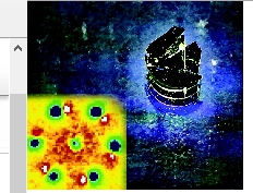
The MSU researchers found that by shooting an ultrafast laser pulse into the material, its properties would change as if it had been chemically “doped.” This process is known as “photo-doping.”
“The material we studied is an unconventional semiconductor made of alternating atomically thin layers of metals and insulators,” said Chong-Yu Ruan, an associate professor of physics and astronomy who led the research effort at MSU. “This combination allows many unusual properties, including highly resistive and also superconducting behaviors to emerge, especially when ‘doped.’”
An ultrafast electron-based imaging technique developed by Ruan and his team at MSU allowed the group to observe the changes in the materials. By varying the wavelengths and intensities of the laser pulses, the researchers were able to observe phases with different properties that are captured on the femtosecond timescale. A femtosecond is 1 quadrillionth, or 1 millionth of 1 billionth, of a second.
“The laser pulses act like dopants that temporarily weaken the glue that binds charges and ions together in the materials at a speed that is ultrafast and allow new electronic phases to spontaneously form to engineer new properties,” Ruan said. “Capturing these processes in the act allows us to understand the physical nature of transformations at the most fundamental level.”
Philip Duxbury, a team member and chairperson of the Department of Physics and Astronomy, said ultrafast photo-doping “has potential applications that could lead to the development of next-generation electronic materials and possibly optically controlled switching devices employing undoped semiconductor materials.”
A semiconductor is a substance that conducts electricity under some conditions but not others, making it a good medium for the control of electrical current. They are used in any number of electronics, including computers.
Other collaborators on the project include the research group of S.D. Mahanti, professor of physics and astronomy at MSU, and the Mercouri Kanatzidis research group at Northwestern University.
The research is supported by Basic Energy Sciences, U.S. Department of Energy.
Share on:


Suggested Items
Real Time with... IPC APEX EXPO 2024: Sustainability in the Industry
04/26/2024 | Real Time with...IPC APEX EXPOGuest Editor Henry Crandall and Chris Nash of Indium Corporation discuss the company's 90th anniversary and its focus on sustainability. They focus on the benefits of sustainable materials, their compatibility, and value propositions. The conversation also highlights how Durafuse LT technology's role in reducing reflow temperatures is leading to significant cost and energy savings. Nash also touches on downstream sustainability efforts such as using recycled materials for packaging.
SMC Korea 2024 to Highlight Semiconductor Materials Trends and Innovations on Industry’s Path to $1 Trillion
04/24/2024 | SEMIWith Korea a major consumer of semiconductor materials and advanced materials a key driver of innovation on the industry’s path to $1 trillion, industry leaders and experts will gather at SMC (Strategic Materials Conference) Korea 2024 on May 29 at the Suwon Convention Center in Gyeonggi-do, South Korea to provide insights into the latest materials developments and trends. Registration is open.
Groundbreaking Ceremony Marks the Beginning of a New Era for Newccess Industrial; The Construction of the MINGXIN Building
04/12/2024 | Newccess IndustrialOn a clear and sunny day in March, the groundbreaking ceremony for the MINGXIN Building took place in Shenzhen, China. This moment marked the official commencement of construction for a project that will reshape the semiconductor materials industry.
The Need for a Holistic Global Sustainability Standard
04/10/2024 | Michael Ford, Aegis SoftwareNo one can deny that the resources of our fragile planet are finite. The environment seems like a third party, subject to constant degradation. We’re acutely aware of the effects of pollution on our climate, and despite our “throw-away” culture, recycling and recovery of materials has remained relatively expensive, even as we use more energy just to survive.
iNEMI Publishes Four Roadmap Topics
04/04/2024 | iNEMIThe International Electronics Manufacturing Initiative (iNEMI) announces the availability of the first roadmap topics in the new iNEMI Roadmap format. Printed circuit boards, sustainable electronics, smart manufacturing, and mmWave materials and test are now available online.