


 The Right Approach: I Hear the Train A Comin'
 It’s Only Common Sense: OCCAM—the Time Is Now
 Marcy's Musings: The Growing Industry
Imec and Panasonic Demonstrate Breakthrough RRAM Cell
July 14, 2015 | ImecEstimated reading time: 2 minutes
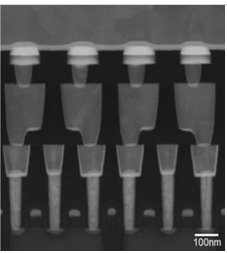
Imec and Panasonic Corp. announced today that they have fabricated a 40nm TaOx-based RRAM (resistive RAM) technology with precise filament positioning and high thermal stability. This breakthrough result paves the way to realizing 28nm embedded applications. The results were presented at this year’s VLSI technology symposium (Kyoto, June 15-19 2015).
One of today’s most promising concepts for scaled memory is RRAM which is based on the electronic (current-or voltage-induced) switching of a resistor element material between two metals. Imec and Panasonic developed a method that overcomes filament instability in RRAM, one of the critical parameters that impacts the memory state during read operation in resistive memory.
The method was realized using a combination of process technologies such as low-damage etching, cell side oxidation, and an innovative encapsulated cell structure with an Ir/Ta2O5/TaOx/TaN stacked film structure featuring a filament at the cell center. With these methods, a 2-Mbit 40nm TaOx-based RRAM cell with precise filament positioning and high thermal stability was achieved. The memory array showed excellent reliability of 100k cycles and 10 years’ retention at 85°C. Additionally, the filament control and thermal stability technologies offer the potential to realize 28nm cell sizes.
Gosia Jurczak, director of imec’s research program on RRAM devices stated: “With these breakthrough results, we have proven the potential of this promising memory concept as embedded nonvolatile memory in 28nm technology node where conventional NOR Flash shows scaling limitations. This result is a confirmation of our leadership position in research and development on resistive memory.”
About Panasonic
Panasonic Corporation is a worldwide leader in the development and engineering of electronic technologies and solutions for customers in residential, non-residential, mobility and personal applications. Since its founding in 1918, the company has expanded globally and now operates around 500 consolidated companies worldwide, recording consolidated net sales of 7.72 trillion yen for the year ended March 31, 2015. Committed to pursuing new value through innovation across divisional lines, the company strives to create a better life and a better world for its customers.
For more information about Panasonic, please visit the company’s website at http://panasonic.net/.
About imec
Imec performs world-leading research in nanoelectronics. Imec leverages its scientific knowledge with the innovative power of its global partnerships in ICT, healthcare and energy. Imec delivers industry-relevant technology solutions. In a unique high-tech environment, its international top talent is committed to providing the building blocks for a better life in a sustainable society. Imec is headquartered in Leuven, Belgium, and has offices in Belgium, the Netherlands, Taiwan, USA, China, India and Japan. Its staff of about 2,200 people includes almost 700 industrial residents and guest researchers. In 2014, imec’s revenue (P&L) totaled 363 million euro. Further information on imec can be found at www.imec.be. Stay up to date about what’s happening at imec with the monthly imec magazine, available for tablets and smartphones (as an app for iOS and Android), or via the website www.imec.be/imecmagazine
Share on:


Suggested Items
Warm Windows and Streamlined Skin Patches – IDTechEx Explores Flexible and Printed Electronics
04/26/2024 | IDTechExFlexible and printed electronics can be integrated into cars and homes to create modern aesthetics that are beneficial and easy to use. From luminous car controls to food labels that communicate the quality of food, the uses of this technology are endless and can upgrade many areas of everyday life.
iNEMI Packaging Tech Topic Series: Role of EDA in Advanced Semiconductor Packaging
04/26/2024 | iNEMIAdvanced semiconductor packaging with heterogenous integration has made on-package integration of multiple chips a crucial part of finding alternatives to transistor scaling. Historically, EDA tools for front-end and back-end design have evolved separately; however, design complexity and the increased number of die-to-die or die-to-substrate interconnections has led to the need for EDA tools that can support integration of overall design planning, implementation, and system analysis in a single cockpit.
Koh Young Showcases Award-winning Inspection Solutions at SMTconnect with SmartRep in Hall 4A.225
04/25/2024 | Koh Young TechnologyKoh Young Technology, the industry leader in True 3D measurement-based inspection solutions, will showcase an array of award-winning inspection and measurement solutions at SMTconnect alongside its sales partner, SmartRep, in booth 4A.225 at NürnbergMesse from June 11-13, 2023. The following offers a glimpse into what Koh Young will present at the tradeshow:
Real Time with… IPC APEX EXPO 2024: Plasmatreat: Innovative Surface Preparation Solutions
04/25/2024 | Real Time with...IPC APEX EXPOIn this interview, Editor Nolan Johnson speaks with Hardev Grewal, CEO and president of Plasmatreat, a developer of atmospheric plasma solutions. Plasmatreat uses clean compressed air and electricity to create plasma, offering environmentally friendly methods for surface preparation. Their technology measures plasma density for process optimization and can remove organic micro-contamination. Nolan and Hardev also discuss REDOX-Tool, a new technology for removing metal oxides.
Nanotechnology Market to Surpass $53.51 Billion by 2031
04/25/2024 | PRNewswireSkyQuest projects that the nanotechnology market will attain a value of USD 53.51 billion by 2031, with a CAGR of 36.4% over the forecast period (2024-2031).