


 The Right Approach: I Hear the Train A Comin'
 It’s Only Common Sense: OCCAM—the Time Is Now
 Marcy's Musings: The Growing Industry
Magnetic Temperature Meter Revealed
July 27, 2015 | CAUEstimated reading time: 1 minute
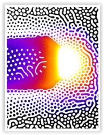
Those who wish to renovate their houses and make them more energy-efficient often use the well-known yellow to blue thermal images to visually identify weak spots applying infra-red measurements. Thermographic imaging is also used in industry for materials testing. Depending on the material, however, the method can result in large measurement errors. Scientists at Kiel University have now developed a technology that visually identifies the slightest temperature differences with high spatial resolution, whatever the material. This new principle competes with other procedures as well, as reported by researchers in the current edition of the scientific journal, Advanced Materials.
In their research, the scientists in Kiel make use of the magnetic properties of a certain material. In experiments, a thin, transparent layer of a garnet compound (garnet is a mineral from the silicates category) is placed on the object to be investigated - in this case, an integrated circuit of a microchip. If the temperature anywhere on the circuit changes even by the slightest amount, the layer of material reacts by changing its magnetic properties. The warmer it becomes, the smaller the magnetisation.
This magnetisation, being different depending on the temperature, can be made visible with a so-called polarisation microscope: polarised light is light that is forced into a certain direction of oscillation (similar to some sunglasses). When it reaches the surface of the thin layer, it is reflected differently, depending on the materials’ magnetisation. A digital, light-sensitive camera captures the reflected light. The magneto-optical images show the temperature distribution in the circuit and the tiny magnetic domains of the material; these are separate areas that have the same polarisation.
The material developed by the physicists in Kiel works as an extremely precise temperature meter. The method can display minimal changes of up to one hundredth of a degree Celsius, which take place in milliseconds, with a resolution of micrometres. Professor Jeffrey McCord, head of the study at the Kiel Institute for Materials Science, is positive that "Our technology therefore opens up brand new possibilities for different thermographic imaging applications." New models of thermographic cameras are conceivable. The new procedure called “Pyro-Magnetic-Optics” could, in particular, make error analysis of electronic components easier and more precise.
The research results were achieved together with scientists from the Russian Tver State University and the Russian Research Institute for Materials Science and Technology.
Share on:


Suggested Items
Real Time with... IPC APEX EXPO 2024: Sustainability in the Industry
04/26/2024 | Real Time with...IPC APEX EXPOGuest Editor Henry Crandall and Chris Nash of Indium Corporation discuss the company's 90th anniversary and its focus on sustainability. They focus on the benefits of sustainable materials, their compatibility, and value propositions. The conversation also highlights how Durafuse LT technology's role in reducing reflow temperatures is leading to significant cost and energy savings. Nash also touches on downstream sustainability efforts such as using recycled materials for packaging.
SMC Korea 2024 to Highlight Semiconductor Materials Trends and Innovations on Industry’s Path to $1 Trillion
04/24/2024 | SEMIWith Korea a major consumer of semiconductor materials and advanced materials a key driver of innovation on the industry’s path to $1 trillion, industry leaders and experts will gather at SMC (Strategic Materials Conference) Korea 2024 on May 29 at the Suwon Convention Center in Gyeonggi-do, South Korea to provide insights into the latest materials developments and trends. Registration is open.
Groundbreaking Ceremony Marks the Beginning of a New Era for Newccess Industrial; The Construction of the MINGXIN Building
04/12/2024 | Newccess IndustrialOn a clear and sunny day in March, the groundbreaking ceremony for the MINGXIN Building took place in Shenzhen, China. This moment marked the official commencement of construction for a project that will reshape the semiconductor materials industry.
The Need for a Holistic Global Sustainability Standard
04/10/2024 | Michael Ford, Aegis SoftwareNo one can deny that the resources of our fragile planet are finite. The environment seems like a third party, subject to constant degradation. We’re acutely aware of the effects of pollution on our climate, and despite our “throw-away” culture, recycling and recovery of materials has remained relatively expensive, even as we use more energy just to survive.
iNEMI Publishes Four Roadmap Topics
04/04/2024 | iNEMIThe International Electronics Manufacturing Initiative (iNEMI) announces the availability of the first roadmap topics in the new iNEMI Roadmap format. Printed circuit boards, sustainable electronics, smart manufacturing, and mmWave materials and test are now available online.