


 The Right Approach: I Hear the Train A Comin'
 It’s Only Common Sense: OCCAM—the Time Is Now
 Marcy's Musings: The Growing Industry
Successful Boron-Doping of Graphene Nanoribbon
August 28, 2015 | University of BaselEstimated reading time: 2 minutes
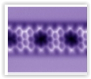
Physicists at the University of Basel succeed in synthesizing boron-doped graphene nanoribbons and characterizing their structural, electronic and chemical properties. The modified material could potentially be used as a sensor for the ecologically damaging nitrogen oxides, scientists report in the latest issue of Nature Communications.
Graphene is one of the most promising materials for improving electronic devices. The two-dimensional carbon sheet exhibits high electron mobility and accordingly has excellent conductivity. Other than usual semiconductors, the material lacks the so-called band gap, an energy range in a solid where no electron states can exist. Therefore, it avoids a situation in which the device is electronically switched off. However, in order to fabricate efficient electronic switches from graphene, it is necessary that the material can be switched ”on” and ”off”.
The solution to this problem lies in trimming the graphene sheet to a ribbon-like shape, named graphene nanoribbon (GNR). Thereby it can be altered to have a band gap whose value is dependent on the width of the shape.
Synthesis on Gold Surface
To tune the band gap in order for the graphene nanoribbons to act like a well-established silicon semiconductor, the ribbons are being doped. To that end, the researchers intentionally introduce impurities into pure material for the purpose of modulating its electrical properties. While nitrogen doping has been realized, boron-doping has remained unexplored. Subsequently, the electronic and chemical properties have stayed unclear thus far.
Prof. Dr. Ernst Meyer and Dr. Shigeki Kawai from the Department of Physics at the University of Basel, assisted by researchers from Japanese and Finnish Universities, have succeeded in synthesizing boron-doped graphene nanoribbons with various widths. They used an on-surface chemical reaction with a newly synthesized precursor molecule on an atomically clean gold surface. The chemical structures were directly resolved by state-of-the-art atomic force microscopy at low temperature.
Towards a Nitrogen Oxide-Sensor
The doped site of the boron atom was unambiguously confirmed and its doping ratio – the number of boron atoms relative to the total number of atoms within the nanoribbon – lay at 4.8 atomic percent. By dosing nitric oxide gas, the chemical property known as the Lewis acidity could also be confirmed.
The doped nitric oxide gas was highly-selectively adsorbed on the boron site. This measurement indicates that the boron-doped graphene nanoribbon can be used for an ultra-high sensitive gas sensor for nitrogen oxides which are currently a hot topic in the industry as being highly damaging to the environment.
Share on:


Suggested Items
Warm Windows and Streamlined Skin Patches – IDTechEx Explores Flexible and Printed Electronics
04/26/2024 | IDTechExFlexible and printed electronics can be integrated into cars and homes to create modern aesthetics that are beneficial and easy to use. From luminous car controls to food labels that communicate the quality of food, the uses of this technology are endless and can upgrade many areas of everyday life.
Book Excerpt: The Printed Circuit Assembler’s Guide to... Factory Analytics
04/24/2024 | I-Connect007 Editorial TeamIn our fast-changing, deeply competitive, and margin-tight industry, factory analytics can be the key to unlocking untapped improvements to guarantee a thriving business. On top of that, electronics manufacturers are facing a tremendous burden to do more with less. If you don't already have a copy of this book, what follows is an excerpt from the introduction chapter of 'The Printed Circuit Assembler’s Guide to... Factory Analytics: Unlocking Efficiency Through Data Insights' to whet your appetite.
Listen Up! The Intricacies of PCB Drilling Detailed in New Podcast Episode
04/25/2024 | I-Connect007In episode 5 of the podcast series, On the Line With: Designing for Reality, Nolan Johnson and Matt Stevenson continue down the manufacturing process, this time focusing on the post-lamination drilling process for PCBs. Matt and Nolan delve into the intricacies of the PCB drilling process, highlighting the importance of hole quality, drill parameters, and design optimization to ensure smooth manufacturing. The conversation covers topics such as drill bit sizes, aspect ratios, vias, challenges in drilling, and ways to enhance efficiency in the drilling department.
Elevating PCB Design Engineering With IPC Programs
04/24/2024 | Cory Blaylock, IPCIn a monumental stride for the electronics manufacturing industry, IPC has successfully championed the recognition of the PCB Design Engineer as an official occupation by the U.S. Department of Labor (DOL). This pivotal achievement not only underscores the critical role of PCB design engineers within the technology landscape, but also marks the beginning of a transformative journey toward nurturing a robust, skilled workforce ready to propel our industry into the future.
Winner of The Science Show Rakett 69 Receives Incap Scholarship
04/24/2024 | IncapThe winner of the Rakett 69 science show, Andri Türkson, who stood out as an electronics enthusiast, received a scholarship from Incap Estonia, along with an internship opportunity in Saaremaa.