


 The Right Approach: I Hear the Train A Comin'
 It’s Only Common Sense: OCCAM—the Time Is Now
 Marcy's Musings: The Growing Industry
Measuring the Behavior of Specific Atoms in Dielectric Materials
October 14, 2015 | NC State UniversityEstimated reading time: 3 minutes
Researchers from North Carolina State University, the National Institute of Standards and Technology (NIST), and UNSW Australia have measured the behavior of specific atoms in dielectric materials when exposed to an electric field. The work advances our understanding of dielectric materials, which are used in a wide variety of applications – from handheld electronics to defibrillators.
“Dielectric materials are insulators that can store and manage electric charge. But we hadn’t yet directly measured how atoms move in dielectric materials in order to store that charge,” says Tedi-Marie Usher, a Ph.D. candidate in materials science and engineering at NC State and lead author of a paper on the work.
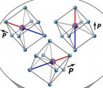
Researchers have measured how the atoms within electrically insulating solids reorient due to an applied electric field. Shown here for Na1/2Bi1/2TiO3, bismuth ions (purple) align along the electric field direction relative to their surrounding titanium ions (blue). Oxygen ions not shown.
To get to the bottom of this problem, the researchers applied voltage to a dielectric material, creating an electric field. They simultaneously bombarded the material with X-rays from a synchrotron at Argonne National Laboratory’s Advanced Photon Source. When the X-rays hit the material, they scatter into a pattern of bright rings. Typically, to figure out the arrangement of atoms in a material, the positions and intensities of these bright rings are analyzed.
However, by applying new mathematical techniques that are more sensitive to the weak (dim) scattered X-rays, the researchers could determine changes in the placement of specific atoms within the crystalline structure of the material. In other words, the researchers could “see” how the atoms moved relative to each other in response to the electric field.
“A good analogy would be that analyzing the bright rings is like examining a skyscraper from far away and determining that each office is 500 square feet. However, by also analyzing the weak X-rays scattered from the sample, we can determine that some offices are 400 square feet and others are 600 square feet, and some have the desk on the east side, and others have the desk on the north side,” says Usher. This is an uncommon approach, because experimenters typically only evaluate the bright rings.
“What’s really new here is that this technique is much more sensitive to the behavior of select atoms relative to their neighboring atoms, rather than looking at an average of all the atoms in a sample,” says Jacob Jones, a professor of materials science and engineering at NC State and corresponding author of the paper.
The work uses a technique called a pair distribution function, which allows researchers to extract information about how atoms are arranged at extremely small length-scales based on the weak intensity X-rays diffracted from a sample. The researchers evaluated three different dielectric materials for this study.
“One of the interesting findings here is that each of the three dielectric materials we tested exhibited very different behaviors at the atomic level – there was no single atomic behavior that accounted for dielectric properties across the materials,” Jones says.
For example, the researchers tested a material called sodium bismuth titanate – a non-toxic material that is thought to be promising for use in dielectric devices. In the absence of an electric field, researchers knew that the bismuth ions are off-center relative to neighboring atoms. But different bismuth ions would be off-center in different directions. However, when an electric field is applied, virtually all of the bismuth ions shifted so they were off-center in the same direction as the electric field.
“Neither of the other dielectric materials exhibited similar behavior,” Usher says. “One of our questions for future work is whether the bismuth behavior we saw in sodium bismuth titanate is consistent across bismuth-based dielectrics.”
“We also want to know how dielectric materials and other complex materials, such as high-entropy alloys, behave at the atomic scale when under mechanical stress,” Jones says.
Share on:


Suggested Items
Real Time with... IPC APEX EXPO 2024: Sustainability in the Industry
04/26/2024 | Real Time with...IPC APEX EXPOGuest Editor Henry Crandall and Chris Nash of Indium Corporation discuss the company's 90th anniversary and its focus on sustainability. They focus on the benefits of sustainable materials, their compatibility, and value propositions. The conversation also highlights how Durafuse LT technology's role in reducing reflow temperatures is leading to significant cost and energy savings. Nash also touches on downstream sustainability efforts such as using recycled materials for packaging.
SMC Korea 2024 to Highlight Semiconductor Materials Trends and Innovations on Industry’s Path to $1 Trillion
04/24/2024 | SEMIWith Korea a major consumer of semiconductor materials and advanced materials a key driver of innovation on the industry’s path to $1 trillion, industry leaders and experts will gather at SMC (Strategic Materials Conference) Korea 2024 on May 29 at the Suwon Convention Center in Gyeonggi-do, South Korea to provide insights into the latest materials developments and trends. Registration is open.
Groundbreaking Ceremony Marks the Beginning of a New Era for Newccess Industrial; The Construction of the MINGXIN Building
04/12/2024 | Newccess IndustrialOn a clear and sunny day in March, the groundbreaking ceremony for the MINGXIN Building took place in Shenzhen, China. This moment marked the official commencement of construction for a project that will reshape the semiconductor materials industry.
The Need for a Holistic Global Sustainability Standard
04/10/2024 | Michael Ford, Aegis SoftwareNo one can deny that the resources of our fragile planet are finite. The environment seems like a third party, subject to constant degradation. We’re acutely aware of the effects of pollution on our climate, and despite our “throw-away” culture, recycling and recovery of materials has remained relatively expensive, even as we use more energy just to survive.
iNEMI Publishes Four Roadmap Topics
04/04/2024 | iNEMIThe International Electronics Manufacturing Initiative (iNEMI) announces the availability of the first roadmap topics in the new iNEMI Roadmap format. Printed circuit boards, sustainable electronics, smart manufacturing, and mmWave materials and test are now available online.