


 The Right Approach: I Hear the Train A Comin'
 It’s Only Common Sense: OCCAM—the Time Is Now
 Marcy's Musings: The Growing Industry
Miniaturizable Magnetic Resonance
November 13, 2015 | University of AlbertaEstimated reading time: 2 minutes
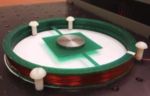
A garnet crystal only one micrometre in diameter was instrumental in a University of Alberta team of physicists creating a route to “lab-on-a-chip” technology for magnetic resonance, a tool to simplify advanced magnetic analysis for device development and interdisciplinary science.
“To most, a gem so tiny would be worthless, but to us, it’s priceless,” says Mark Freeman, University of Alberta physics professor and Canada Research Chair in condensed matter physics. “It was the perfect testbed for this new method.”
In the new method of measuring magnetic resonance, published in the November 13, 2015 issue of the journal Science, the signal is a mechanical twisting motion, detected with light. The new approach is more naturally suited to miniaturization than the current method, which creates an electrical signal by induction. In fact, the entire magnetic sensor unit created with the new technology can fit on a chip as small as one square centimetre.
“Our discovery makes the case that magnetic resonance is in essence both a mechanical and magnetic phenomenon on account of magnetic dipoles possessing angular momentum,” says Freeman, noting that the concept of magnetism makes more sense when you consider its mechanical properties. “Magnetism needs better spin doctors than it has had. Everything in the world is magnetic on some level, so the possibilities for scientific applications of this new technique are endless.”
The discovery opens up a world of possible miniaturized platforms for health care, technology, energy, environmental monitoring, and space exploration. Explains Freeman, “There are immediate applications in physics, Earth sciences, and engineering, but we have only looked at electron spin resonance. Proton spin resonance is the next big step that will open up applications in chemistry and biology.”
Mark Freeman (seated), with Fatemeh Fani Sani (middle row left), Joseph Losby (top right) and team members have discovered a route to lab-on-a-chip technology for magnetic resonance, a tool to simplify advanced magnetic analysis for device development and interdisciplinary science.
To foster the development of these applications, Freeman’s team plans to openly share the information about how to execute this technique, feeding the current maker movement. It was important to the team not to patent this discovery—as is often the pressure for scientists conducting these types of discoveries—but instead to publish their findings in a scientific journal to provide open-source access that will advance the field. “Ultimately, the way science makes progress is through people sharing discoveries,” says Freeman, adding that he hopes others will adapt the technology for their own needs.
Freeman, who worked for IBM before coming to the University of Alberta, believes that chip-based miniaturizable mechanical devices—by virtue of their small scale and superior performance—will come to replace some electronic sensors in devices like smart phones and on space exploration probes. “It’s an elegant solution to a challenging problem, simple but not obvious,” says Freeman, who has been working on the experimental challenge solved in this paper for the past two decades. “Working in condensed matter physics is like having the best seat at an awe-inspiring parade of progress.”
Share on:


Suggested Items
Warm Windows and Streamlined Skin Patches – IDTechEx Explores Flexible and Printed Electronics
04/26/2024 | IDTechExFlexible and printed electronics can be integrated into cars and homes to create modern aesthetics that are beneficial and easy to use. From luminous car controls to food labels that communicate the quality of food, the uses of this technology are endless and can upgrade many areas of everyday life.
iNEMI Packaging Tech Topic Series: Role of EDA in Advanced Semiconductor Packaging
04/26/2024 | iNEMIAdvanced semiconductor packaging with heterogenous integration has made on-package integration of multiple chips a crucial part of finding alternatives to transistor scaling. Historically, EDA tools for front-end and back-end design have evolved separately; however, design complexity and the increased number of die-to-die or die-to-substrate interconnections has led to the need for EDA tools that can support integration of overall design planning, implementation, and system analysis in a single cockpit.
Koh Young Showcases Award-winning Inspection Solutions at SMTconnect with SmartRep in Hall 4A.225
04/25/2024 | Koh Young TechnologyKoh Young Technology, the industry leader in True 3D measurement-based inspection solutions, will showcase an array of award-winning inspection and measurement solutions at SMTconnect alongside its sales partner, SmartRep, in booth 4A.225 at NürnbergMesse from June 11-13, 2023. The following offers a glimpse into what Koh Young will present at the tradeshow:
Real Time with… IPC APEX EXPO 2024: Plasmatreat: Innovative Surface Preparation Solutions
04/25/2024 | Real Time with...IPC APEX EXPOIn this interview, Editor Nolan Johnson speaks with Hardev Grewal, CEO and president of Plasmatreat, a developer of atmospheric plasma solutions. Plasmatreat uses clean compressed air and electricity to create plasma, offering environmentally friendly methods for surface preparation. Their technology measures plasma density for process optimization and can remove organic micro-contamination. Nolan and Hardev also discuss REDOX-Tool, a new technology for removing metal oxides.
Nanotechnology Market to Surpass $53.51 Billion by 2031
04/25/2024 | PRNewswireSkyQuest projects that the nanotechnology market will attain a value of USD 53.51 billion by 2031, with a CAGR of 36.4% over the forecast period (2024-2031).