


 Material Insight: The Dielectric Constant of PCB Materials
 American Made Advocacy: What About the Rest of the Technology Stack?
 It’s Only Common Sense: Great Ideas From John Mitchell’s Book on Hiring Habits
Coming to a Monitor Near You: A Defect-free, Molecule-thick Film
November 27, 2015 | University of California - BerkeleyEstimated reading time: 2 minutes
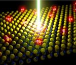
An emerging class of atomically thin materials known as monolayer semiconductors has generated a great deal of buzz in the world of materials science. Monolayers hold promise in the development of transparent LED displays, ultra-high efficiency solar cells, photo detectors and nanoscale transistors. Their downside? The films are notoriously riddled with defects, killing their performance.
But now a research team, led by engineers at the University of California, Berkeley, and Lawrence Berkeley National Laboratory, has found a simple way to fix these defects through the use of an organic superacid. The chemical treatment led to a dramatic 100-fold increase in the material's photoluminescence quantum yield, a ratio describing the amount of light generated by the material versus the amount of energy put in. The greater the emission of light, the higher the quantum yield and the better the material quality.
The researchers enhanced the quantum yield for molybdenum disulfide, or MoS2, from less than 1 percent up to 100 percent by dipping the material into a superacid called bistriflimide, or TFSI.
Their findings, to be published in the Nov. 27 issue of Science, opens the door to the practical application of monolayer materials, such as MoS2, in optoelectronic devices and high-performance transistors. MoS2 is a mere seven-tenths of a nanometer thick. For comparison, a strand of human DNA is 2.5 nanometers in diameter.
"Traditionally, the thinner the material, the more sensitive it is to defects," said principal investigator Ali Javey, UC Berkeley professor of electrical engineering and computer sciences and a faculty scientist at Berkeley Lab. "This study presents the first demonstration of an optoelectronically perfect monolayer, which previously had been unheard of in a material this thin."
The researchers looked to superacids because, by definition, they are solutions with a propensity to "give" protons, often in the form of hydrogen atoms, to other substances. This chemical reaction, called protonation, has the effect of filling in for the missing atoms at the site of defects as well as removing unwanted contaminants stuck on the surface, the researchers said.
Co-lead authors of the paper are UC Berkeley Ph.D. student Matin Amani, visiting Ph.D. student Der-Hsien Lien and postdoctoral fellow Daisuke Kiriya.
Page 1 of 2
Share on:


Suggested Items
Material Insight: The Dielectric Constant of PCB Materials
05/17/2024 | Dr. Preeya Kuray -- Column: Material InsightIn the world of PCB design, miniaturization can be achieved by using low dielectric constant (Dk) materials. Low Dk materials can allow for a reduction in thickness while maintaining a given trace width, leading to lower transmission loss and higher density circuitry.
IPC APEX EXPO: Some Thoughts About Growth
05/16/2024 | Dan Feinberg, I-Connect007After two and a half days of wandering the aisles at IPC APEX EXPO 2024, for the first time, I almost felt like I was exploring CES. There were so many booths and exhibits that I could describe, but I’d like to focus on the growth and huge value of this event, which has expanded well beyond just the growing and impressive exhibit show floor.
The Shaughnessy Report: Unlock Your High-speed Material Constraints
05/15/2024 | Andy Shaughnessy -- Column: The Shaughnessy ReportThe world of PCB materials used to be a fairly simple one. It was divided into two groups: the “traditional” laminates, often called FR-4, and the high-speed laminates developed especially for high-speed PCBs. These were two worlds that usually didn’t collide. But then traditional laminates started getting better, and high-speed designers and design engineers took notice and started to reconsider what FR-4 could be used for.
Breaking High-speed Material Constraints: Design007 Magazine — May 2024
05/14/2024 | I-Connect007 Editorial TeamDo you need specialty materials for your high-speed designs? Maybe not. Improvements in resins mean designers of high-speed boards can sometimes use traditional laminate systems instead of high-speed materials, saving time and money while streamlining the fab process. In the May 2024 issue of Design007 Magazine, our contributors explain how to avoid overconstraining your materials when working with high-speed boards.
Indium Experts to Present at Electronics in Harsh Environments SMTA Conference
05/13/2024 | Indium Corporationndium Corporation Technical Manager for Europe, Africa, and the Middle East, Karthik Vijay, will deliver a technical presentation and Indium Corporation Senior Technologist, Dr. Ronald Lasky, will deliver both a workshop and technical presentation at the Electronics in Harsh Environments SMTA Conference on May 14-16 in Copenhagen, Denmark.