


 Material Insight: The Dielectric Constant of PCB Materials
 American Made Advocacy: What About the Rest of the Technology Stack?
 It’s Only Common Sense: Great Ideas From John Mitchell’s Book on Hiring Habits
New Approaches for Hybrid Solar Cells
December 8, 2015 | Technical University of MunichEstimated reading time: 3 minutes
Using a new procedure researchers at the Technical University of Munich (TUM) and the Ludwig Maximillians University of Munich (LMU) can now produce extremely thin and robust, yet highly porous semiconductor layers. A very promising material – for small, light-weight, flexible solar cells, for example, or electrodes improving the performance of rechargeable batteries.
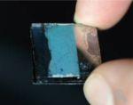
The coating on the wafer that Professor Thomas Fässler, chair of Inorganic Chemistry with a Focus on Novel Materials at TU Munich, holds in his hands glitters like an opal. And it has amazing properties: It is hard as a crystal, exceptionally thin and – since it is highly porous – light as a feather.
By integrating suitable organic polymers into the pores of the material, the scientists can custom tailor the electrical properties of the ensuing hybrid material. The design not only saves space, it also creates large interface surfaces that improve overall effectiveness.
“You can imagine our raw material as a porous scaffold with a structure akin to a honeycomb. The walls comprise inorganic, semiconducting germanium, which can produce and store electric charges. Since the honeycomb walls are extremely thin, charges can flow along short paths,” explains Fässler.
The new design: bottom-up instead of top-down
But, to transform brittle, hard germanium into a flexible and porous layer the researchers had to apply a few tricks. Traditionally, etching processes are used to structure the surface of germanium. However, this top-down approach is difficult to control on an atomic level. The new procedure solves this problem.
Together with his team, Fässler established a synthesis methodology to fabricate the desired structures very precisely and reproducibly. The raw material is germanium with atoms arranged in clusters of nine. Since these clusters are electrically charged, they repel each other as long as they are dissolved. Netting only takes place when the solvent is evaporated.
This can be easily achieved by applying heat of 500 °C or it can be chemically induced, by adding germanium chloride, for example. By using other chlorides like phosphorous chloride the germanium structures can be easily doped. This allows the researchers to directly adjust the properties of the resulting nanomaterials in a very targeted manner.
Page 1 of 2
Share on:


Suggested Items
Material Insight: The Dielectric Constant of PCB Materials
05/17/2024 | Dr. Preeya Kuray -- Column: Material InsightIn the world of PCB design, miniaturization can be achieved by using low dielectric constant (Dk) materials. Low Dk materials can allow for a reduction in thickness while maintaining a given trace width, leading to lower transmission loss and higher density circuitry.
IPC APEX EXPO: Some Thoughts About Growth
05/16/2024 | Dan Feinberg, I-Connect007After two and a half days of wandering the aisles at IPC APEX EXPO 2024, for the first time, I almost felt like I was exploring CES. There were so many booths and exhibits that I could describe, but I’d like to focus on the growth and huge value of this event, which has expanded well beyond just the growing and impressive exhibit show floor.
The Shaughnessy Report: Unlock Your High-speed Material Constraints
05/15/2024 | Andy Shaughnessy -- Column: The Shaughnessy ReportThe world of PCB materials used to be a fairly simple one. It was divided into two groups: the “traditional” laminates, often called FR-4, and the high-speed laminates developed especially for high-speed PCBs. These were two worlds that usually didn’t collide. But then traditional laminates started getting better, and high-speed designers and design engineers took notice and started to reconsider what FR-4 could be used for.
Breaking High-speed Material Constraints: Design007 Magazine — May 2024
05/14/2024 | I-Connect007 Editorial TeamDo you need specialty materials for your high-speed designs? Maybe not. Improvements in resins mean designers of high-speed boards can sometimes use traditional laminate systems instead of high-speed materials, saving time and money while streamlining the fab process. In the May 2024 issue of Design007 Magazine, our contributors explain how to avoid overconstraining your materials when working with high-speed boards.
Indium Experts to Present at Electronics in Harsh Environments SMTA Conference
05/13/2024 | Indium Corporationndium Corporation Technical Manager for Europe, Africa, and the Middle East, Karthik Vijay, will deliver a technical presentation and Indium Corporation Senior Technologist, Dr. Ronald Lasky, will deliver both a workshop and technical presentation at the Electronics in Harsh Environments SMTA Conference on May 14-16 in Copenhagen, Denmark.