


 The Right Approach: I Hear the Train A Comin'
 It’s Only Common Sense: OCCAM—the Time Is Now
 Marcy's Musings: The Growing Industry
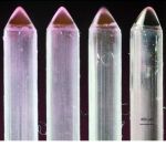
Microelectromechanical systems — or MEMS — were a $12 billion business in 2014. But that market is dominated by just a handful of devices, such as the accelerometers that reorient the screens of most smartphones.
That’s because manufacturing MEMS has traditionally required sophisticated semiconductor fabrication facilities, which cost tens of millions of dollars to build. Potentially useful MEMS have languished in development because they don’t have markets large enough to justify the initial capital investment in production.
Two recent papers from researchers at MIT’s Microsystems Technologies Laboratories offer hope that that might change. In one, the researchers show that a MEMS-based gas sensor manufactured with a desktop device performs at least as well as commercial sensors built at conventional production facilities.
In the other paper, they show that the central component of the desktop fabrication device can itself be built with a 3-D printer. Together, the papers suggest that a widely used type of MEMS gas sensor could be produced at one-hundredth the cost with no loss of quality.
The researchers’ fabrication device sidesteps many of the requirements that make conventional MEMS manufacture expensive. “The additive manufacturing we’re doing is based on low temperature and no vacuum,” says Luis Fernando Velásquez-García, a principal research scientist in MIT’s Microsystems Technology Laboratories and senior author on both papers. “The highest temperature we’ve used is probably 60 degrees Celsius. In a chip, you probably need to grow oxide, which grows at around 1,000 degrees Celsius. And in many cases the reactors require these high vacuums to prevent contamination. We also make the devices very quickly. The devices we reported are made in a matter of hours from beginning to end.”
Welcome resistance
For years, Velásquez-García has been researching manufacturing techniques that involve dense arrays of emitters that eject microscopic streams of fluid when subjected to strong electric fields. For the gas sensors, Velásquez-García and Anthony Taylor, a visiting researcher from the British company Edwards Vacuum, use so-called “internally fed emitters.” These are emitters with cylindrical bores that allow fluid to pass through them.
In this case, the fluid contained tiny flakes of graphene oxide. Discovered in 2004, graphene is an atom-thick form of carbon with remarkable electrical properties. Velásquez-García and Taylor used their emitters to spray the fluid in a prescribed pattern on a silicon substrate. The fluid quickly evaporated, leaving a coating of graphene oxide flakes only a few tens of nanometers thick. Page 1 of 2
Share on:


Suggested Items
Real Time with… IPC APEX EXPO 2024: Tools, Training, and Trends in Manufacturing Engineering
04/25/2024 | Real Time with...IPC APEX EXPOGuest Editor Kelly Dack and Product Specialist Erik Bateham of Polar Instruments discuss Polar's latest technology, including their role in aiding manufacturing engineers. They highlight the advanced capabilities of Polar's tools and the critical role of signal integrity analysis, as well as the importance of accurate modeling in board manufacturing. Polar's unique training approach and demonstration contact details are also explored.
TTM Celebrates the Grand Opening of Its First Manufacturing Facility in Penang
04/25/2024 | TTM Technologies, Inc.TTM Technologies, Inc., a leading global manufacturer of technology solutions including mission systems, radio frequency (RF) components and RF microwave/microelectronic assemblies, and quick-turn and technologically advanced printed circuit boards (PCBs), officially opened its first manufacturing plant in Penang, Malaysia with an investment of USD200 million (approximately RM958 million).
Listen Up! The Intricacies of PCB Drilling Detailed in New Podcast Episode
04/25/2024 | I-Connect007In episode 5 of the podcast series, On the Line With: Designing for Reality, Nolan Johnson and Matt Stevenson continue down the manufacturing process, this time focusing on the post-lamination drilling process for PCBs. Matt and Nolan delve into the intricacies of the PCB drilling process, highlighting the importance of hole quality, drill parameters, and design optimization to ensure smooth manufacturing. The conversation covers topics such as drill bit sizes, aspect ratios, vias, challenges in drilling, and ways to enhance efficiency in the drilling department.
Elevating PCB Design Engineering With IPC Programs
04/24/2024 | Cory Blaylock, IPCIn a monumental stride for the electronics manufacturing industry, IPC has successfully championed the recognition of the PCB Design Engineer as an official occupation by the U.S. Department of Labor (DOL). This pivotal achievement not only underscores the critical role of PCB design engineers within the technology landscape, but also marks the beginning of a transformative journey toward nurturing a robust, skilled workforce ready to propel our industry into the future.
Fujitsu, METRON Collaborate to Drive ESG Success
04/24/2024 | JCN NewswireFujitsu Limited and METRON SAS, a French cleantech company specializing in energy management solutions for industrial decarbonization, today announced a strategic initiative to contribute to the realization of carbon neutrality in the manufacturing industry.