


 Material Insight: The Dielectric Constant of PCB Materials
 American Made Advocacy: What About the Rest of the Technology Stack?
 It’s Only Common Sense: Great Ideas From John Mitchell’s Book on Hiring Habits
Nanoworld 'Snow Blowers' Carve Straight Channels in Semiconductor Surfaces
December 29, 2015 | NISTEstimated reading time: 2 minutes
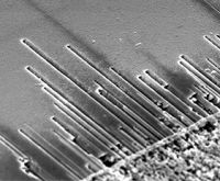
In the nanoworld, tiny particles of gold can operate like snow blowers, churning through surface layers of an important class of semiconductors to dig unerringly straight paths. The surprising trenching capability, reported by scientists from the National Institute of Standards and Technology (NIST) and IBM, is an important addition to the toolkit of nature-supplied “self-assembly” methods that researchers aim to harness for making useful devices.
Foreseeable applications include integrating lasers, sensors, wave guides and other optical components into so-called lab-on-a-chip devices now used for disease diagnosis, screening experimental materials and drugs, DNA forensics and more. Easy to control, the new gold-catalyzed process for creating patterns of channels with nanoscale dimensions could help to spawn entirely new technologies fashioned from ensembles of ultra-small structures.
Preliminary research results that began as lemons—a contaminant-caused failure that impeded the expected formation of nanowires—eventually turned into lemonade when scanning electron microscope images revealed long, straight channels.
“We were disappointed, at first,” says NIST research chemist Babak Nikoobakht. “Then we figured out that water was the contaminant in the process—a problem that turned out to be a good thing.”
That’s because, as determined in subsequent experiments, the addition of water vapor served to transform gold nanoparticles into channel diggers, rather than the expected wire makers. Beginning with studies on the semiconductor indium phosphide, the team teased out the chemical mechanisms and necessary conditions underpinning the surface-etching process.
First, they patterned the surface of the semiconductor by selectively coating it with a gold layer only a few nanometers thick. Upon heating, the film breaks up into tiny particles that become droplets. The underlying indium phosphide dissolves into the gold nanoparticles above, creating a gold alloy. Then, heated water vapor is introduced into the system. At temperatures below 300 degrees Celsius (572 degrees Fahrenheit), the tiny gold-alloy particles, now swathed with water molecules, etch nanoscale pits into the indium phosphide.
Page 1 of 2
Share on:


Suggested Items
Avnet Launches QCS6490 Vision-AI Development Kit
05/17/2024 | AvnetThe QCS6490 Vision-AI Development Kit from Avnet enables engineering teams to rapidly prototype hardware, application software and AI enablement for multi-camera, high-performance, Edge AI-enabled custom embedded products.
Standard of Excellence: Collaboration—The Right Path to Innovation
05/15/2024 | Anaya Vardya -- Column: Standard of ExcellenceNow more than ever, as new and innovative technologies for printed circuit boards are in demand, we need collaboration between PCB designers, fabricators, and assemblers. Close partnerships with PCB designers and assemblers are key to developing and producing PCBs with boards with new and innovative technology. These collaborative partnerships, along with the partnership with the end customers, are more critical than ever before.
Listen Up: Popular Podcast Series Returns With Discussion of Electroless Copper
05/16/2024 | I-Connect007In the latest episode of the podcast series, On the Line With: Designing for Reality, Nolan Johnson returns to Sunstone Circuits in Mulino, OR, to continue down the manufacturing process with Matt Stevenson.
Breaking High-speed Material Constraints: Design007 Magazine — May 2024
05/14/2024 | I-Connect007 Editorial TeamDo you need specialty materials for your high-speed designs? Maybe not. Improvements in resins mean designers of high-speed boards can sometimes use traditional laminate systems instead of high-speed materials, saving time and money while streamlining the fab process. In the May 2024 issue of Design007 Magazine, our contributors explain how to avoid overconstraining your materials when working with high-speed boards.
IDENTCO Highlights Automation Capabilities and PCB Labeling at PCB East
05/13/2024 | IDENTCOIDENTCO – a manufacturer of high-performance labeling solutions for the power equipment, electronics, transportation, and general industrial sector – will highlight its automation capabilities and PCB labeling solutions at PCB East, June 4-7 in Boxborough, MA, Booth #301.