


 Material Insight: The Dielectric Constant of PCB Materials
 American Made Advocacy: What About the Rest of the Technology Stack?
 It’s Only Common Sense: Great Ideas From John Mitchell’s Book on Hiring Habits
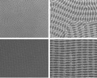
Since the 1960s, computer chips have been built using a process called photolithography. But in the past five years, chip features have gotten smaller than the wavelength of light, which has required some ingenious modifications of photolithographic processes. Keeping up the rate of circuit miniaturization that we’ve come to expect — as predicted by Moore’s Law — will eventually require new manufacturing techniques.
Block copolymers, molecules that spontaneously self-assemble into useful shapes, are one promising alternative to photolithography. In a new paper in the journal Nature Communications, MIT researchers describe the first technique for stacking layers of block-copolymer wires such that the wires in one layer naturally orient themselves perpendicularly to those in the layer below.
The ability to easily produce such “mesh structures” could make self-assembly a much more practical way to manufacture memory, optical chips, and even future generations of computer processors.
“There is previous work on fabricating a mesh structure — for example our work,” says Amir Tavakkoli, a postdoc in MIT’s Research Laboratory of Electronics and one of three first authors on the new paper. “We used posts that we had fabricated by electron-beam lithography, which is time consuming. But here, we don’t use the electron-beam lithography. We use the first layer of block copolymer as a template to self-assemble another layer of block copolymer on top of it.”
Tavakkoli’s co-first-authors on the paper are Sam Nicaise, a graduate student in electrical engineering, and Karim Gadelrab, a graduate student in materials science and engineering. The senior authors are Alfredo Alexander-Katz, the Walter Henry Gale Associate Professor of Materials Science and Engineering; Caroline Ross, the Toyota Professor of Materials Science and Engineering; and Karl Berggren, a professor of electrical engineering.
Page 1 of 3
Share on:


Suggested Items
Material Insight: The Dielectric Constant of PCB Materials
05/17/2024 | Dr. Preeya Kuray -- Column: Material InsightIn the world of PCB design, miniaturization can be achieved by using low dielectric constant (Dk) materials. Low Dk materials can allow for a reduction in thickness while maintaining a given trace width, leading to lower transmission loss and higher density circuitry.
IPC APEX EXPO: Some Thoughts About Growth
05/16/2024 | Dan Feinberg, I-Connect007After two and a half days of wandering the aisles at IPC APEX EXPO 2024, for the first time, I almost felt like I was exploring CES. There were so many booths and exhibits that I could describe, but I’d like to focus on the growth and huge value of this event, which has expanded well beyond just the growing and impressive exhibit show floor.
The Shaughnessy Report: Unlock Your High-speed Material Constraints
05/15/2024 | Andy Shaughnessy -- Column: The Shaughnessy ReportThe world of PCB materials used to be a fairly simple one. It was divided into two groups: the “traditional” laminates, often called FR-4, and the high-speed laminates developed especially for high-speed PCBs. These were two worlds that usually didn’t collide. But then traditional laminates started getting better, and high-speed designers and design engineers took notice and started to reconsider what FR-4 could be used for.
Breaking High-speed Material Constraints: Design007 Magazine — May 2024
05/14/2024 | I-Connect007 Editorial TeamDo you need specialty materials for your high-speed designs? Maybe not. Improvements in resins mean designers of high-speed boards can sometimes use traditional laminate systems instead of high-speed materials, saving time and money while streamlining the fab process. In the May 2024 issue of Design007 Magazine, our contributors explain how to avoid overconstraining your materials when working with high-speed boards.
Indium Experts to Present at Electronics in Harsh Environments SMTA Conference
05/13/2024 | Indium Corporationndium Corporation Technical Manager for Europe, Africa, and the Middle East, Karthik Vijay, will deliver a technical presentation and Indium Corporation Senior Technologist, Dr. Ronald Lasky, will deliver both a workshop and technical presentation at the Electronics in Harsh Environments SMTA Conference on May 14-16 in Copenhagen, Denmark.