


 The Right Approach: I Hear the Train A Comin'
 It’s Only Common Sense: OCCAM—the Time Is Now
 Marcy's Musings: The Growing Industry
Engineering Material Magic
February 15, 2016 | University of UtahEstimated reading time: 2 minutes
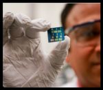
University of Utah engineers have discovered a new kind of 2D semiconducting material for electronics that opens the door for much speedier computers and smartphones that also consume a lot less power.
The semiconductor, made of the elements tin and oxygen, or tin monoxide (SnO), is a layer of 2D material only one atom thick, allowing electrical charges to move through it much faster than conventional 3D materials such as silicon. This material could be used in transistors, the lifeblood of all electronic devices such as computer processors and graphics processors in desktop computers and mobile devices. The material was discovered by a team led by University of Utah materials science and engineering associate professor Ashutosh Tiwari. A paper describing the research was published online Monday, Feb. 15, 2016 in the journal, Advanced Electronic Materials. The paper, which also will be the cover story on the printed version of the journal, was co-authored by University of Utah materials science and engineering doctoral students K. J. Saji and Kun Tian, and Michael Snure of the Wright-Patterson Air Force Research Lab near Dayton, Ohio.
Transistors and other components used in electronic devices are currently made of 3D materials such as silicon and consist of multiple layers on a glass substrate. But the downside to 3D materials is that electrons bounce around inside the layers in all directions.
The benefit of 2D materials, which is an exciting new research field that has opened up only about five years ago, is that the material is made of one layer the thickness of just one or two atoms. Consequently, the electrons "can only move in one layer so it's much faster," says Tiwari.
While researchers in this field have recently discovered new types of 2D material such as graphene, molybdenun disulfide and borophene, they have been materials that only allow the movement of N-type, or negative, electrons. In order to create an electronic device, however, you need semiconductor material that allows the movement of both negative electrons and positive charges known as "holes." The tin monoxide material discovered by Tiwari and his team is the first stable P-type 2D semiconductor material ever in existence.
"Now we have everything -- we have P-type 2D semiconductors and N-type 2D semiconductors," he says. "Now things will move forward much more quickly."
Now that Tiwari and his team have discovered this new 2D material, it can lead to the manufacturing of transistors that are even smaller and faster than those in use today. A computer processor is comprised of billions of transistors, and the more transistors packed into a single chip, the more powerful the processor can become.
Transistors made with Tiwari's semiconducting material could lead to computers and smartphones that are more than 100 times faster than regular devices. And because the electrons move through one layer instead of bouncing around in a 3D material, there will be less friction, meaning the processors will not get as hot as normal computer chips. They also will require much less power to run, a boon for mobile electronics that have to run on battery power. Tiwari says this could be especially important for medical devices such as electronic implants that will run longer on a single battery charge.
"The field is very hot right now, and people are very interested in it," Tiwari says. "So in two or three years we should see at least some prototype device."
Share on:


Suggested Items
Real Time with... IPC APEX EXPO 2024: Sustainability in the Industry
04/26/2024 | Real Time with...IPC APEX EXPOGuest Editor Henry Crandall and Chris Nash of Indium Corporation discuss the company's 90th anniversary and its focus on sustainability. They focus on the benefits of sustainable materials, their compatibility, and value propositions. The conversation also highlights how Durafuse LT technology's role in reducing reflow temperatures is leading to significant cost and energy savings. Nash also touches on downstream sustainability efforts such as using recycled materials for packaging.
SMC Korea 2024 to Highlight Semiconductor Materials Trends and Innovations on Industry’s Path to $1 Trillion
04/24/2024 | SEMIWith Korea a major consumer of semiconductor materials and advanced materials a key driver of innovation on the industry’s path to $1 trillion, industry leaders and experts will gather at SMC (Strategic Materials Conference) Korea 2024 on May 29 at the Suwon Convention Center in Gyeonggi-do, South Korea to provide insights into the latest materials developments and trends. Registration is open.
Groundbreaking Ceremony Marks the Beginning of a New Era for Newccess Industrial; The Construction of the MINGXIN Building
04/12/2024 | Newccess IndustrialOn a clear and sunny day in March, the groundbreaking ceremony for the MINGXIN Building took place in Shenzhen, China. This moment marked the official commencement of construction for a project that will reshape the semiconductor materials industry.
The Need for a Holistic Global Sustainability Standard
04/10/2024 | Michael Ford, Aegis SoftwareNo one can deny that the resources of our fragile planet are finite. The environment seems like a third party, subject to constant degradation. We’re acutely aware of the effects of pollution on our climate, and despite our “throw-away” culture, recycling and recovery of materials has remained relatively expensive, even as we use more energy just to survive.
iNEMI Publishes Four Roadmap Topics
04/04/2024 | iNEMIThe International Electronics Manufacturing Initiative (iNEMI) announces the availability of the first roadmap topics in the new iNEMI Roadmap format. Printed circuit boards, sustainable electronics, smart manufacturing, and mmWave materials and test are now available online.