


 The Right Approach: I Hear the Train A Comin'
 It’s Only Common Sense: OCCAM—the Time Is Now
 Marcy's Musings: The Growing Industry
Nanolaser for Information Technology
February 16, 2016 | Technical University of MunichEstimated reading time: 3 minutes
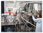
Physicists at the Technical University of Munich (TUM) have developed a nanolaser, a thousand times thinner than a human hair. Thanks to an ingenious process, the nanowire lasers grow right on a silicon chip, making it possible to produce high-performance photonic components cost-effectively. This will pave the way for fast and efficient data processing with light in the future.
Ever smaller, ever faster, ever cheaper – since the start of the computer age the performance of processors has doubled on average every 18 months. 50 years ago already, Intel co-founder Gordon E. Moore prognosticated this astonishing growth in performance. And Moore’s law seems to hold true to this day.
But the miniaturization of electronics is now reaching its physical limits. “Today already, transistors are merely a few nanometers in size. Further reductions are horrendously expensive,” says Professor Jonathan Finley, Director of the Walter Schottky Institute at TUM. “Improving performance is achievable only by replacing electrons with photons, i.e. particles of light.”
Photonics – the silver bullet of miniaturization
Data transmission and processing with light has the potential of breaking the barriers of current electronics. In fact, the first silicon-based photonics chips already exist. However, the sources of light for the transmission of data must be attached to the silicon in complicated and elaborate manufacturing processes. Researchers around the world are thus searching for alternative approaches.
Scientists at the TU Munich have now succeeded in this endeavor: Dr. Gregor Koblmüller at the Department of Semiconductor Quantum-Nanosystems has, in collaboration with Jonathan Finley, developed a process to deposit nanolasers directly onto silicon chips. A patent for the technology is pending.
Growing a III-V semiconductor onto silicon requires tenacious experimentation. “The two materials have different lattice parameters and different coefficients of thermal expansion. This leads to strain,” explains Koblmüller. “For example, conventional planar growth of gallium arsenide onto a silicon surface results therefore in a large number of defects.”
The TUM team solved this problem in an ingenious way: By depositing nanowires that are freestanding on silicon their footprints are merely a few square nanometers. The scientists could thus preclude the emerging of defects in the GaAs material.
Atom by atom to a nanowire
But how do you turn a nanowire into a vertical-cavity laser? To generate coherent light, photons must be reflected at the top and bottom ends of the wire, thereby amplifying the light until it reaches the desired threshold for lasing.
To fulfil these conditions, the researchers had to develop a simple, yet sophisticated solution: “The interface between gallium arsenide and silicon does not reflect light sufficiently. We thus built in an additional mirror – a 200 nanometer thick silicon oxide layer that we evaporated onto the silicon,” explains Benedikt Mayer, doctoral candidate in the team led by Koblmüller and Finley. “Tiny holes can then be etched into the mirror layer. Using epitaxy, the semiconductor nanowires can then be grown atom for atom out of these holes.”
Only once the wires protrude beyond the mirror surface they may grow laterally – until the semiconductor is thick enough to allow photons to jet back and forth to allow stimulated emission and lasing. “This process is very elegant because it allows us to position the nanowire lasers directly also onto waveguides in the silicon chip,” says Koblmüller.
Basic research on the path to applications
Currently, the new gallium arsenide nanowire lasers produce infrared light at a predefined wavelength and under pulsed excitation. “In the future we want to modify the emission wavelength and other laser parameters to better control temperature stability and light propagation under continuous excitation within the silicon chips,” adds Finley.
The team has just published its first successes in this direction. And they have set their sights firmly on their next goal: “We want to create an electric interface so that we can operate the nanowires under electrical injection instead of relying on external lasers,” explains Koblmüller.
“The work is an important prerequisite for the development of high-performance optical components in future computers,” sums up Finley. “We were able to demonstrate that manufacturing silicon chips with integrated nanowire lasers is possible.”
The research was funded by the German Research Foundation (DFG) through the TUM Institute for Advanced Study, the Excellence Cluster Nanosystems Initiative Munich (NIM) and the International Graduate School of Science and Engineering (IGSSE) of the TUM, as well as by IBM through an international postgraduate program.
Share on:


Suggested Items
CACI Awarded $1.3 Billion Task Order to Provide Communications and Information Technology Expertise
04/26/2024 | CACI International Inc.CACI International Inc announced that it has been awarded a five-year task order worth a total estimated value of $1.3 billion to provide communications and information technology expertise to U.S. European Command (USEUCOM) and U.S. Africa Command (USAFRICOM).
Intel Gaudi, Xeon and AI PC Accelerate Meta Llama 3 GenAI Workloads
04/22/2024 | Intel CorporationMeta launched Meta Llama 3, its next-generation large language model (LLM). Effective on launch day, Intel has validated its AI product portfolio for the first Llama 3 8B and 70B models across Intel® Gaudi® accelerators, Intel® Xeon® processors, Intel® Core™ Ultra processors and Intel® Arc™ graphics.
Cadence Unveils Palladium Z3 and Protium X3 Systems
04/18/2024 | Cadence Design SystemsThe Palladium Z3 and Protium X3 systems offer increased capacity, and scale from job sizes of 16 million gates up to 48 billion gates, so the largest SoCs can be tested as a whole rather than just partial models, ensuring proper functionality and performance.
IDTechEx Explores the Role of 3D Cu-Cu Hybrid Bonding in Powering Future HPC and AI Products
04/18/2024 | PRNewswireSemiconductor packaging has evolved from traditional 1D PCB levels to cutting-edge 3D hybrid bonding at the wafer level, achieving interconnecting pitches as small as single micrometers and over 1000 GB/s bandwidth. Key parameters, including Power, Performance, Area, and Cost, are crucial considerations
Northrop Grumman Honors Calumet Electronics with Supplier Excellence Award
04/17/2024 | Calumet ElectronicsNorthrop Grumman Corporation has recognized Calumet Electronics during the company’s 2024 Supplier Excellence Awards for “exceptional performance and unwavering commitment to delivering with excellence.” Calumet is one of 70 suppliers recognized from across the globe. In its award category of “Supplier Strategic Excellence,” Calumet was honored alongside global corporations such as Amazon Web Services, Dell Technologies, and Eaton Corporation.