


 The Right Approach: I Hear the Train A Comin'
 It’s Only Common Sense: OCCAM—the Time Is Now
 Marcy's Musings: The Growing Industry
Breakthrough for Lab-on-a-chip Material
February 24, 2016 | KTH Royal Institute of TechnologyEstimated reading time: 2 minutes
Researchers at KTH Royal Institute of Technology have developed a new polymer suited for photostructuring — a technique for creating micro-scale shapes. The discovery opens new possibilities for medical diagnostics, biophotonics and 3D printing.
The so-called off-stoichiometry thiol-enes (OSTE) polymer was developed at KTH specifically to meet the need for a material suitable for both experimental prototyping and large-scale manufacturing of labs-on-a-chip — or, miniaturized bioanalytical laboratories.
"It can be very useful in a variety of applications such as near-patient diagnostic tools," says one of the developers, Tommy Haraldsson, docent in the department Micro and Nanosystems at KTH.
One of the unique qualities of OSTE polymer is that its surface is chemically reactive without adding anything or preparing the surface in a special way. Now, another benefit has been revealed.
In the February issue of Nature publishing group journal Microsystems and Nanoengineering, the authors report the discovery that upon exposure to UV light, the molecules of the polymer arrange themselves in a manner that significantly enhances photostructuring.
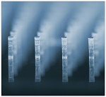
Photostructuring is a technique by which UV light is used to solidify micro-scale 3D shapes in liquid polymer. "These microstructures can guide light, such as with waveguides. Or they can be used to control fluid flow, such as with microfluidics channels," says Gaspard Pardon, a post-doc researcher in Micro and Nanosystems at KTH.
Up until now, the major class of polymers to which the KTH material belongs, thiol-ene copolymers, has been considered to be inappropriate for photostructuring.
"With this new understanding of the underlying mechanisms and material properties available, we can also anticipate future exciting applications," Pardon says.
"Biophotonics is one such area," Pardon says. Biophotonics harnesses light and other forms of radiant energy to understand the inner workings of cells and tissues. This approach enables researchers to see, measure, analyze and manipulate biological materials in ways never before possible.
"We also started testing the 3D printing of our new material. By producing 3D structures that have the material's special surface chemical properties, it would allow the polymer to be used in a variety of new applications," he says.
The OSTE polymer was developed over the last five years to bridge the “lab-to-fab-gap”, and create an alternative to suboptimal off-the-shelf materials that are now used for conceptual lab-on-a-chip device development. The predominant materials used today are known to have poor mechanical or chemical properties, such as absorption of small molecules and difficulties with permanent surface modification.
With the KTH material however it is possible to easily add different layers of material or to modify the surface properties for handling microscopic flows of fluids, without using glue or otherwise treating the material surface. Another possibility is that the material allows simple change in the surface's wettability and chemistry.
"We can also integrate sensitive biomaterials and bioreagents, and the manufacturing cost is potentially reduced because the material is so easy to work with," Pardon says.
Share on:


Suggested Items
Real Time with… IPC APEX EXPO 2024: Exploring the Future of Surface Finishes
04/25/2024 | Real Time with...IPC APEX EXPOJoe McGurran, product marketing director for MKS Atotech, looks into the future of surface finishes, discussing less nickel, reduced thickness, technologies influencing HDI and UHDI, and the benefits of nickel-free surface finishes. He also touches on popular finishes like ENIG and palladium immersion gold and discusses the value proposition of making a change.
Designer’s Notebook: What Designers Need to Know About Manufacturing, Part 2
04/24/2024 | Vern Solberg -- Column: Designer's NotebookThe printed circuit board (PCB) is the primary base element for providing the interconnect platform for mounting and electrically joining electronic components. When assessing PCB design complexity, first consider the component area and board area ratio. If the surface area for the component interface is restricted, it may justify adopting multilayer or multilayer sequential buildup (SBU) PCB fabrication to enable a more efficient sub-surface circuit interconnect.
IDTechEx Report Unveils 3D Electronics Status and Opportunities
04/22/2024 | PRNewswire3D electronics is an emerging manufacturing approach that enables electronics to be integrated within or onto the surface of objects. 3D electronic manufacturing techniques empower new features, including mass customizability, greater integration, and improved sustainability in the electronics industry.
NASA, Japan Advance Space Cooperation, Sign Agreement for Lunar Rover
04/11/2024 | NASANASA Administrator Bill Nelson and Japan’s Minister of Education, Culture, Sports, Science and Technology (MEXT) Masahito Moriyama have signed an agreement to advance sustainable human exploration of the Moon.
Lockheed Martin Conducts Historic LRASM Flight Test
04/04/2024 | Lockheed MartinThe U.S. Navy in partnership with Lockheed Martin [NYSE: LMT] successfully conducted a historic Long-Range Anti-Ship Missile (LRASM) flight test with four missiles simultaneously in flight.