


 The Right Approach: I Hear the Train A Comin'
 It’s Only Common Sense: OCCAM—the Time Is Now
 Marcy's Musings: The Growing Industry
Researchers Stack the Odds for Novel Optoelectronic 2D Materials
March 3, 2016 | ORNLEstimated reading time: 4 minutes
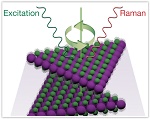
Stacking layers of nanometer-thin semiconducting materials at different angles is a new approach to designing the next generation of energy-efficient transistors and solar cells. The atoms in each layer are arranged in hexagonal arrays. When two layers are stacked and rotated, atoms from one layer overlap with those in the other layer and can form an infinite number of overlapping patterns, like the Moiré patternsthat result when two screens are overlaid and one is rotated on top of the other. Theoretical calculations predict excellent electronic and optical properties for some stacking patterns, but practically, how can these patterns be made and characterized?
Recently a team led by researchers from the Department of Energy’s Oak Ridge National Laboratory used the vibrations between two layers to decipher their stacking patterns. The team employed a method called low-frequency Raman spectroscopy to measure how the layers vibrate with respect to each other and compared the frequencies of the measured vibrations with their theoretically predicted values. Their study provides a platform for engineering two-dimensional (2D) materials with optical and electronic properties that strongly depend on stacking configurations. The findings are published in ACS Nano,a journal of the American Chemical Society.
“Low-frequency Raman spectroscopy, in combination with first-principles modeling, offers a quick and easy approach to reveal complex stacking configurations in the twisted bilayers of a promising semiconductor, without relying on other expensive and time-consuming experimental techniques,” said co-lead author Liangbo Liang, a Wigner Fellow at ORNL. “We are the first to show that low-frequency Raman spectra can be used as fingerprints to characterize the relative layer stacking in semiconducting 2D materials.”
In Raman scattering, an optical method for probing atomic vibrations, a material scatters monochromatic light from a laser. Whereas conventional Raman spectroscopy may probe more than approximately 3 trillion atomic vibrations per second, low-frequency Raman spectroscopy detects vibrations that are an order of magnitude slower. The low-frequency technique is sensitive to weak attractive forces between layers, called van der Waals coupling. It can provide crucial insight about layer thickness and stacking—aspects that govern fundamental properties of 2D materials.
“This work combines state-of-the art synthesis and processing of 2D materials, their unique spectroscopic characterization, and data interpretation using first-principles theory,” said co-lead author Alex Puretzky. “High-resolution Raman spectroscopy that can probe low-frequency modes requires specialized instrumentation, and only a few places around the world have such a capability together with advanced synthesis and characterization tools, and theory and computational modeling expertise. The Center for Nanophase Materials Sciences at ORNL is among them.”
Page 1 of 2
Share on:


Suggested Items
Real Time with... IPC APEX EXPO 2024: Sustainability in the Industry
04/26/2024 | Real Time with...IPC APEX EXPOGuest Editor Henry Crandall and Chris Nash of Indium Corporation discuss the company's 90th anniversary and its focus on sustainability. They focus on the benefits of sustainable materials, their compatibility, and value propositions. The conversation also highlights how Durafuse LT technology's role in reducing reflow temperatures is leading to significant cost and energy savings. Nash also touches on downstream sustainability efforts such as using recycled materials for packaging.
SMC Korea 2024 to Highlight Semiconductor Materials Trends and Innovations on Industry’s Path to $1 Trillion
04/24/2024 | SEMIWith Korea a major consumer of semiconductor materials and advanced materials a key driver of innovation on the industry’s path to $1 trillion, industry leaders and experts will gather at SMC (Strategic Materials Conference) Korea 2024 on May 29 at the Suwon Convention Center in Gyeonggi-do, South Korea to provide insights into the latest materials developments and trends. Registration is open.
Groundbreaking Ceremony Marks the Beginning of a New Era for Newccess Industrial; The Construction of the MINGXIN Building
04/12/2024 | Newccess IndustrialOn a clear and sunny day in March, the groundbreaking ceremony for the MINGXIN Building took place in Shenzhen, China. This moment marked the official commencement of construction for a project that will reshape the semiconductor materials industry.
The Need for a Holistic Global Sustainability Standard
04/10/2024 | Michael Ford, Aegis SoftwareNo one can deny that the resources of our fragile planet are finite. The environment seems like a third party, subject to constant degradation. We’re acutely aware of the effects of pollution on our climate, and despite our “throw-away” culture, recycling and recovery of materials has remained relatively expensive, even as we use more energy just to survive.
iNEMI Publishes Four Roadmap Topics
04/04/2024 | iNEMIThe International Electronics Manufacturing Initiative (iNEMI) announces the availability of the first roadmap topics in the new iNEMI Roadmap format. Printed circuit boards, sustainable electronics, smart manufacturing, and mmWave materials and test are now available online.