


 Material Insight: The Dielectric Constant of PCB Materials
 American Made Advocacy: What About the Rest of the Technology Stack?
 It’s Only Common Sense: Great Ideas From John Mitchell’s Book on Hiring Habits
Researchers Stack the Odds for Novel Optoelectronic 2D Materials
March 3, 2016 | ORNLEstimated reading time: 4 minutes
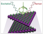
Stacking layers of nanometer-thin semiconducting materials at different angles is a new approach to designing the next generation of energy-efficient transistors and solar cells. The atoms in each layer are arranged in hexagonal arrays. When two layers are stacked and rotated, atoms from one layer overlap with those in the other layer and can form an infinite number of overlapping patterns, like the Moiré patternsthat result when two screens are overlaid and one is rotated on top of the other. Theoretical calculations predict excellent electronic and optical properties for some stacking patterns, but practically, how can these patterns be made and characterized?
Recently a team led by researchers from the Department of Energy’s Oak Ridge National Laboratory used the vibrations between two layers to decipher their stacking patterns. The team employed a method called low-frequency Raman spectroscopy to measure how the layers vibrate with respect to each other and compared the frequencies of the measured vibrations with their theoretically predicted values. Their study provides a platform for engineering two-dimensional (2D) materials with optical and electronic properties that strongly depend on stacking configurations. The findings are published in ACS Nano,a journal of the American Chemical Society.
“Low-frequency Raman spectroscopy, in combination with first-principles modeling, offers a quick and easy approach to reveal complex stacking configurations in the twisted bilayers of a promising semiconductor, without relying on other expensive and time-consuming experimental techniques,” said co-lead author Liangbo Liang, a Wigner Fellow at ORNL. “We are the first to show that low-frequency Raman spectra can be used as fingerprints to characterize the relative layer stacking in semiconducting 2D materials.”
In Raman scattering, an optical method for probing atomic vibrations, a material scatters monochromatic light from a laser. Whereas conventional Raman spectroscopy may probe more than approximately 3 trillion atomic vibrations per second, low-frequency Raman spectroscopy detects vibrations that are an order of magnitude slower. The low-frequency technique is sensitive to weak attractive forces between layers, called van der Waals coupling. It can provide crucial insight about layer thickness and stacking—aspects that govern fundamental properties of 2D materials.
“This work combines state-of-the art synthesis and processing of 2D materials, their unique spectroscopic characterization, and data interpretation using first-principles theory,” said co-lead author Alex Puretzky. “High-resolution Raman spectroscopy that can probe low-frequency modes requires specialized instrumentation, and only a few places around the world have such a capability together with advanced synthesis and characterization tools, and theory and computational modeling expertise. The Center for Nanophase Materials Sciences at ORNL is among them.”
Page 1 of 2
Share on:


Suggested Items
Material Insight: The Dielectric Constant of PCB Materials
05/17/2024 | Dr. Preeya Kuray -- Column: Material InsightIn the world of PCB design, miniaturization can be achieved by using low dielectric constant (Dk) materials. Low Dk materials can allow for a reduction in thickness while maintaining a given trace width, leading to lower transmission loss and higher density circuitry.
IPC APEX EXPO: Some Thoughts About Growth
05/16/2024 | Dan Feinberg, I-Connect007After two and a half days of wandering the aisles at IPC APEX EXPO 2024, for the first time, I almost felt like I was exploring CES. There were so many booths and exhibits that I could describe, but I’d like to focus on the growth and huge value of this event, which has expanded well beyond just the growing and impressive exhibit show floor.
The Shaughnessy Report: Unlock Your High-speed Material Constraints
05/15/2024 | Andy Shaughnessy -- Column: The Shaughnessy ReportThe world of PCB materials used to be a fairly simple one. It was divided into two groups: the “traditional” laminates, often called FR-4, and the high-speed laminates developed especially for high-speed PCBs. These were two worlds that usually didn’t collide. But then traditional laminates started getting better, and high-speed designers and design engineers took notice and started to reconsider what FR-4 could be used for.
Breaking High-speed Material Constraints: Design007 Magazine — May 2024
05/14/2024 | I-Connect007 Editorial TeamDo you need specialty materials for your high-speed designs? Maybe not. Improvements in resins mean designers of high-speed boards can sometimes use traditional laminate systems instead of high-speed materials, saving time and money while streamlining the fab process. In the May 2024 issue of Design007 Magazine, our contributors explain how to avoid overconstraining your materials when working with high-speed boards.
Indium Experts to Present at Electronics in Harsh Environments SMTA Conference
05/13/2024 | Indium Corporationndium Corporation Technical Manager for Europe, Africa, and the Middle East, Karthik Vijay, will deliver a technical presentation and Indium Corporation Senior Technologist, Dr. Ronald Lasky, will deliver both a workshop and technical presentation at the Electronics in Harsh Environments SMTA Conference on May 14-16 in Copenhagen, Denmark.