


 The Right Approach: I Hear the Train A Comin'
 It’s Only Common Sense: OCCAM—the Time Is Now
 Marcy's Musings: The Growing Industry
Nanotechnologists at UT Make Orientation of Magnetism Adjustable in New Materials
March 8, 2016 | University of TwenteEstimated reading time: 2 minutes
Nanotechnologists at the UT research institute MESA+ are now able to create materials in which they can influence and precisely control the orientation of the magnetism at will. An interlayer just 0.4 nanometres thick is the key to this success. The materials present a range of interesting possibilities, such as a new way of creating computer memory as well as spintronics applications – a new form of electronics that works on the basis of magnetism instead of electricity. The research was published today in the leading scientific journal Nature Materials.
Nanotechnologists at the University of Twente are specialized in creating new materials. Thanks to the top-level facilities at the MESA+ NanoLab they are able to combine materials as they wish, with the ability to control the material composition down to atom level. In particular, they specialize in creating materials composed of extremely thin layers, sometimes just one atom thick.
Computer memory
In research published today in the scientific journal Nature Materials, they show their ability to create new materials within which they can precisely and locally control the orientation of the magnetism. This opens the way to new possibilities of creating computer memory. Moreover, this method of creating materials is interesting for spintronics, a new form of electronics that does not utilize the movement of charges but instead the magnetic properties of a material. This not only makes electronics very fast and efficient, but also allows them to be produced in extremely small dimensions.
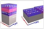
Interlayer
In the course of this research the scientists stacked up various thin layers of Perovskite materials. By placing an extremely thin interlayer of just 0.4 nanometres between the layers (a nanometre is a million times smaller than a millimetre), it becomes possible to influence the orientation of the magnetism in the individual Perovskite layers as desired, whereby the orientation of the magnetism in the bottom layer, for instance, is perpendicular to that of the layer above. By varying the location where the interlayer is applied, it becomes possible to select the local orientation of the magnetism anywhere in the material. This is an essential property for new forms of computer memory and for spintronics applications. This effect was already known for much thicker layers, but never before had researchers demonstrated that the orientation of the magnetism can be controlled so precisely with extremely thin layers, too.
Research
The research has been conducted by scientists of the MESA+ research group Inorganic Materials Science in collaboration with colleagues from other institutes, including the University of Antwerp (Belgium), the University of British Columbia (Canada) and TU Wien (Vienna, Austria). Within the research project, the Twente-based researchers were responsible for coordination and for creating the materials. The colleague researchers from Antwerp visualized the materials and were able to image even the smallest atoms in the material. The Canadian researchers created a magnetic cross-section of the material, while the Austrian researchers handled the theoretical calculations.
Share on:


Suggested Items
Real Time with... IPC APEX EXPO 2024: Sustainability in the Industry
04/26/2024 | Real Time with...IPC APEX EXPOGuest Editor Henry Crandall and Chris Nash of Indium Corporation discuss the company's 90th anniversary and its focus on sustainability. They focus on the benefits of sustainable materials, their compatibility, and value propositions. The conversation also highlights how Durafuse LT technology's role in reducing reflow temperatures is leading to significant cost and energy savings. Nash also touches on downstream sustainability efforts such as using recycled materials for packaging.
SMC Korea 2024 to Highlight Semiconductor Materials Trends and Innovations on Industry’s Path to $1 Trillion
04/24/2024 | SEMIWith Korea a major consumer of semiconductor materials and advanced materials a key driver of innovation on the industry’s path to $1 trillion, industry leaders and experts will gather at SMC (Strategic Materials Conference) Korea 2024 on May 29 at the Suwon Convention Center in Gyeonggi-do, South Korea to provide insights into the latest materials developments and trends. Registration is open.
Groundbreaking Ceremony Marks the Beginning of a New Era for Newccess Industrial; The Construction of the MINGXIN Building
04/12/2024 | Newccess IndustrialOn a clear and sunny day in March, the groundbreaking ceremony for the MINGXIN Building took place in Shenzhen, China. This moment marked the official commencement of construction for a project that will reshape the semiconductor materials industry.
The Need for a Holistic Global Sustainability Standard
04/10/2024 | Michael Ford, Aegis SoftwareNo one can deny that the resources of our fragile planet are finite. The environment seems like a third party, subject to constant degradation. We’re acutely aware of the effects of pollution on our climate, and despite our “throw-away” culture, recycling and recovery of materials has remained relatively expensive, even as we use more energy just to survive.
iNEMI Publishes Four Roadmap Topics
04/04/2024 | iNEMIThe International Electronics Manufacturing Initiative (iNEMI) announces the availability of the first roadmap topics in the new iNEMI Roadmap format. Printed circuit boards, sustainable electronics, smart manufacturing, and mmWave materials and test are now available online.