


 The Right Approach: I Hear the Train A Comin'
 It’s Only Common Sense: OCCAM—the Time Is Now
 Marcy's Musings: The Growing Industry
Plasma Processing Technique Takes SNS Accelerator to New Energy Highs
March 9, 2016 | ORNLEstimated reading time: 2 minutes
A novel technique known as in-situ plasma processing is helping scientists get more neutrons and better data for their experiments at the Spallation Neutron Source at the Department of Energy's Oak Ridge National Laboratory.
"Plasma cleaning is a well-known technique in electrostatics," said ORNL's Research Accelerator Division Director Kevin Jones, "but it has not been applied before to superconducting cavities, and there are some interesting tricks that you have to develop and apply in order to make it all work."
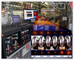
SNS's linear accelerator, or linac, features a set of 20-plus cryomodules--large, barrel-shaped capsules, necessary for focusing and accelerating the proton beam. Inside each cryomodule are 3-4 niobium cavity strings, accordion-like components bathed in liquid helium that keeps the cavities cold to aid in generating very strong electrical fields that drive the beam's acceleration.
Jones explained that over the years trace amounts of hydrocarbon contamination builds up inside the niobium cavities, lessening their ability to sustain high electrical fields, and thus decreasing the beam's potential energy. The conventional response to the problem would be to physically take the cryomodules offline, disassemble them, remove the contamination using ultra-pure water or a chemical rinse, and then finally put everything back together--a labor intensive and costly process.
ORNL staff scientist Marc Doleans and postdoctoral researcher Puneet Tyagi found a better solution. Together they led a team of technicians from SNS's Superconducting Linac Systems Group that undertook a program of rigorous surface science and bench-top experiments with room-temperature cavities that culminated in a series of trial procedures using an offline, spare cryomodule.
"Essentially what they're doing is using hot plasma to burn off the hydrocarbons on and just below the surfaces [inside the niobium cavities]. They're using an inert gas with a few percent of oxygen. Basically, the oxygen gobbles up all the bad atoms off the surface of the niobium, and afterwards everything gets pumped out as a gas," Jones said. "It's just cleaning off junk on the surface--kind of like polishing your car."
After the trial procedures were complete, the team tested the cryomodule's performance and saw a significant improvement. That gave the go ahead for the team to carry out the in-situ procedure in the accelerator tunnel during the facility's scheduled winter maintenance outage.
As expected, the procedure was a success. Not only did the team do in 3 weeks what would have taken 6 to 8 months using conventional methods, but furthermore, subsequent testing recorded an energy gain of 11 million electron volts (MeV). The increase from 938 to 949 MeV is a big step forward, according to Jones.
In addition to a few other upgrades, he said, "Today we're running the accelerator at the highest beam energy ever in neutron production at 957 MeV. If we use this procedure on, say, 5 more cryomodules, and we get equivalent gains, we can easily get up to operating at our design energy of 1,000 MeV."
Ramping up the power to the SNS proton beam enables the production of more neutrons for the thousands of scientists who visit the DOE Office of Science User Facility to conduct research.
The work is already generating a lot of buzz, and it's being viewed very positively, Jones says. In addition to their recent publication in the scientific journals NIM A and Applied Surface Science, the team has been asked to collaborate with other national labs conducting research into superconducting accelerators.
"This is high-profile stuff," Jones said. "It saves us an enormous amount of money, effort, and time in improving the performance of those cavities, and our investment has been worth every penny."
Share on:


Suggested Items
Real Time with… IPC APEX EXPO 2024: Exploring the Future of Surface Finishes
04/25/2024 | Real Time with...IPC APEX EXPOJoe McGurran, product marketing director for MKS Atotech, looks into the future of surface finishes, discussing less nickel, reduced thickness, technologies influencing HDI and UHDI, and the benefits of nickel-free surface finishes. He also touches on popular finishes like ENIG and palladium immersion gold and discusses the value proposition of making a change.
Designer’s Notebook: What Designers Need to Know About Manufacturing, Part 2
04/24/2024 | Vern Solberg -- Column: Designer's NotebookThe printed circuit board (PCB) is the primary base element for providing the interconnect platform for mounting and electrically joining electronic components. When assessing PCB design complexity, first consider the component area and board area ratio. If the surface area for the component interface is restricted, it may justify adopting multilayer or multilayer sequential buildup (SBU) PCB fabrication to enable a more efficient sub-surface circuit interconnect.
IDTechEx Report Unveils 3D Electronics Status and Opportunities
04/22/2024 | PRNewswire3D electronics is an emerging manufacturing approach that enables electronics to be integrated within or onto the surface of objects. 3D electronic manufacturing techniques empower new features, including mass customizability, greater integration, and improved sustainability in the electronics industry.
NASA, Japan Advance Space Cooperation, Sign Agreement for Lunar Rover
04/11/2024 | NASANASA Administrator Bill Nelson and Japan’s Minister of Education, Culture, Sports, Science and Technology (MEXT) Masahito Moriyama have signed an agreement to advance sustainable human exploration of the Moon.
Lockheed Martin Conducts Historic LRASM Flight Test
04/04/2024 | Lockheed MartinThe U.S. Navy in partnership with Lockheed Martin [NYSE: LMT] successfully conducted a historic Long-Range Anti-Ship Missile (LRASM) flight test with four missiles simultaneously in flight.