


 The Right Approach: I Hear the Train A Comin'
 It’s Only Common Sense: OCCAM—the Time Is Now
 Marcy's Musings: The Growing Industry
Researchers Develop Highly Efficient Hollow Copper Electrodes
March 9, 2016 | University of TwenteEstimated reading time: 3 minutes
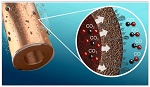
Scientists at the University of Twente research institute MESA+ have developed an electrode in the form of a hollow porous copper fibre which is able to convert carbon dioxide (CO2) into carbon monoxide (CO) extremely efficiently. In principle the invention enables a wide variety of industrial processes, for example in the steel industry, to be made more sustainable. The researchers have applied for a patent on their invention, and their research results have been published in the scientific journal Nature Communications.
Researchers at the University of Twente have developed a hollow copper fibre which can be used to convert CO2 into CO with a very high efficiency. The fibre, which serves as an electrode, is provided with countless minute pores. If the fibre is placed in a bath of water, a voltage potential applied, and CO2 pumped in, the CO2 is converted into CO as it passes out through these pores.
Efficiency and selectivity
The principle is straightforward but the efficiency and selectivity of the reaction are surprisingly high, in part because the electrode provides a huge surface area on which the reaction can take place. An important innovation is the optimized interface between gas, fluid and copper particles, allowing the very efficient supply of CO2 and removal of the product, CO. Conversion takes place at about ten times the rate when using the most advanced copper electrodes currently available, while the selectivity (expressed as the percentage of electrons that actually convert CO2 into CO) is 85%, compared to 35% in current copper electrodes. The newly developed electrode also performs better than electrodes made of expensive precious metals such as gold or silver.
Manufacturing process
The fibres are manufactured in the following way. Small copper particles are added to a polymer solution. This solution is guided through a small, ring-shaped slit in a water bath, in which the polymer solution solidifies into the form of a thin hollow fibre. A thermal treatment is then employed to remove the polymer and partially fuse the copper particles. The result is a copper oxide fibre. Reacting this with hydrogen at a high temperature yields the final product: a hollow, porous copper fibre with a diameter of 1.5mm and a wall thickness of 0.1mm.
Because this manufacturing technique is based on the way polymeric hollow-fibre membranes are currently constructed on a very large scale, e.g. for kidney dialysis equipment, the researchers involved believe it will be relatively easy to produce the new electrode on a commercial scale.
Page 1 of 2
Share on:


Suggested Items
Designer’s Notebook: What Designers Need to Know About Manufacturing, Part 2
04/24/2024 | Vern Solberg -- Column: Designer's NotebookThe printed circuit board (PCB) is the primary base element for providing the interconnect platform for mounting and electrically joining electronic components. When assessing PCB design complexity, first consider the component area and board area ratio. If the surface area for the component interface is restricted, it may justify adopting multilayer or multilayer sequential buildup (SBU) PCB fabrication to enable a more efficient sub-surface circuit interconnect.
Insulectro’s 'Storekeepers' Extend Their Welcome to Technology Village at IPC APEX EXPO
04/03/2024 | InsulectroInsulectro, the largest distributor of materials for use in the manufacture of PCBs and printed electronics, welcomes attendees to its TECHNOLOGY VILLAGE during this year’s IPC APEX EXPO at the Anaheim Convention Center, April 9-11, 2024.
ENNOVI Introduces a New Flexible Circuit Production Process for Low Voltage Connectivity in EV Battery Cell Contacting Systems
04/03/2024 | PRNewswireENNOVI, a mobility electrification solutions partner, introduces a more advanced and sustainable way of producing flexible circuits for low voltage signals in electric vehicle (EV) battery cell contacting systems.
Heavy Copper PCBs: Bridging the Gap Between Design and Fabrication, Part 1
04/01/2024 | Yash Sutariya, Saturn Electronics ServicesThey call me Sparky. This is due to my talent for getting shocked by a variety of voltages and because I cannot seem to keep my hands out of power control cabinets. While I do not have the time to throw the knife switch to the off position, that doesn’t stop me from sticking screwdrivers into the fuse boxes. In all honesty, I’m lucky to be alive. Fortunately, I also have a talent for building high-voltage heavy copper circuit boards. Since this is where I spend most of my time, I can guide you through some potential design for manufacturability (DFM) hazards you may encounter with heavy copper design.
Trouble in Your Tank: Supporting IC Substrates and Advanced Packaging, Part 5
03/19/2024 | Michael Carano -- Column: Trouble in Your TankDirect metallization systems based on conductive graphite or carbon dispersion are quickly gaining acceptance worldwide. Indeed, the environmental and productivity gains one can achieve with these processes are outstanding. In today’s highly competitive and litigious environment, direct metallization reduces costs associated with compliance, waste treatment, and legal issues related to chemical exposure. What makes these processes leaders in the direct metallization space?