


 The Right Approach: I Hear the Train A Comin'
 It’s Only Common Sense: OCCAM—the Time Is Now
 Marcy's Musings: The Growing Industry
DNA 'Origami' Could Help Build Faster, Cheaper Computer Chips
March 14, 2016 | American Chemical Society (ACS)Estimated reading time: 3 minutes
Electronics manufacturers constantly hunt for ways to make faster, cheaper computer chips, often by cutting production costs or by shrinking component sizes. Now, researchers report that DNA, the genetic material of life, might help accomplish this goal when it is formed into specific shapes through a process reminiscent of the ancient art of paper folding.
The researchers present their work today at the 251st National Meeting & Exposition of the American Chemical Society (ACS). ACS, the world's largest scientific society, is holding the meeting here through Thursday. It features more than 12,500 presentations on a wide range of science topics.
"We would like to use DNA's very small size, base-pairing capabilities and ability to self-assemble, and direct it to make nanoscale structures that could be used for electronics," Adam T. Woolley, Ph.D., says. He explains that the smallest features on chips currently produced by electronics manufacturers are 14 nanometers wide. That's more than 10 times larger than the diameter of single-stranded DNA, meaning that this genetic material could form the basis for smaller-scale chips.
"The problem, however, is that DNA does not conduct electricity very well," he says. "So we use the DNA as a scaffold and then assemble other materials on the DNA to form electronics."
To design computer chips similar in function to those that Silicon Valley churns out, Woolley, in collaboration with Robert C. Davis, Ph.D., and John N. Harb, Ph.D., at Brigham Young University, is building on other groups' prior work on DNA origami and DNA nanofabrication.
The most familiar form of DNA is a double helix, which consists of two single strands of DNA. Complementary bases on each strand pair up to connect the two strands, much like rungs on a twisted ladder. But to create a DNA origami structure, researchers begin with a long single strand of DNA. The strand is flexible and floppy, somewhat like a shoelace. Scientists then mix it with many other short strands of DNA -- known as "staples" -- that use base pairing to pull together and crosslink multiple, specific segments of the long strand to form a desired shape.
However, Woolley's team isn't content with merely replicating the flat shapes typically used in traditional two-dimensional circuits. "With two dimensions, you are limited in the density of components you can place on a chip," Woolley explains. "If you can access the third dimension, you can pack in a lot more components."
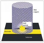
Kenneth Lee, an undergraduate who works with Woolley, has built a 3-D, tube-shaped DNA origami structure that sticks up like a smokestack from substrates, such as silicon, that will form the bottom layer of their chip. Lee has been experimenting with attaching additional short strands of DNA to fasten other components such as nano-sized gold particles at specific sites on the inside of the tube. The researchers' ultimate goal is to place such tubes, and other DNA origami structures, at particular sites on the substrate. The team would also link the structures' gold nanoparticles with semiconductor nanowires to form a circuit. In essence, the DNA structures serve as girders on which to build an integrated circuit.
Lee is currently testing the characteristics of the tubular DNA. He plans to attach additional components inside the tube, with the eventual aim of forming a semiconductor.
Woolley notes that a conventional chip fabrication facility costs more than $1 billion, in part because the equipment necessary to achieve the minuscule dimensions of chip components is expensive and because the multi-step manufacturing process requires hundreds of instruments. In contrast, a facility that harnesses DNA's knack for self-assembly would likely entail much lower start-up funding, he states. "Nature works on a large scale, and it is really good at assembling things reliably and efficiently," he says. "If that could be applied in making circuits for computers, there's potential for huge cost savings."
Share on:


Suggested Items
KIC’s Miles Moreau to Present Profiling Basics and Best Practices at SMTA Wisconsin Chapter PCBA Profile Workshop
01/25/2024 | KICKIC, a renowned pioneer in thermal process and temperature measurement solutions for electronics manufacturing, announces that Miles Moreau, General Manager, will be a featured speaker at the SMTA Wisconsin Chapter In-Person PCBA Profile Workshop.
The Drive Toward UHDI and Substrates
09/20/2023 | I-Connect007 Editorial TeamPanasonic’s Darren Hitchcock spoke with the I-Connect007 Editorial Team on the complexities of moving toward ultra HDI manufacturing. As we learn in this conversation, the number of shifting constraints relative to traditional PCB fabrication is quite large and can sometimes conflict with each other.
Standard Of Excellence: The Products of the Future
09/19/2023 | Anaya Vardya -- Column: Standard of ExcellenceIn my last column, I discussed cutting-edge innovations in printed circuit board technology, focusing on innovative trends in ultra HDI, embedded passives and components, green PCBs, and advanced substrate materials. This month, I’m following up with the products these new PCB technologies are destined for. Why do we need all these new technologies?
Experience ViTrox's State-of-the-Art Offerings at SMTA Guadalajara 2023 Presented by Sales Channel Partner—SMTo Engineering
09/18/2023 | ViTroxViTrox, which aims to be the world’s most trusted technology company, is excited to announce that our trusted Sales Channel Partner (SCP) in Mexico, SMTo Engineering, S.A. de C.V., will be participating in SMTA Guadalajara Expo & Tech Forum. They will be exhibiting in Booth #911 from the 25th to the 26th of October 2023, at the Expo Guadalajara in Jalisco, Mexico.
Intel Unveils Industry-Leading Glass Substrates to Meet Demand for More Powerful Compute
09/18/2023 | IntelIntel announced one of the industry’s first glass substrates for next-generation advanced packaging, planned for the latter part of this decade.