


 The Right Approach: I Hear the Train A Comin'
 It’s Only Common Sense: OCCAM—the Time Is Now
 Marcy's Musings: The Growing Industry
Replacement for Silicon Devices Looms Big with ORNL Discovery
March 18, 2016 | ORNLEstimated reading time: 1 minute
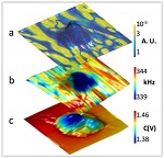
Two-dimensional electronic devices could inch closer to their ultimate promise of low power, high efficiency and mechanical flexibility with a processing technique developed at the Department of Energy's Oak Ridge National Laboratory.
A team led by Olga Ovchinnikova of ORNL's Center for Nanophase Materials Sciences Division used a helium ion microscope, an atomic-scale "sandblaster," on a layered ferroelectric surface of a bulk copper indium thiophosphate. The result, detailed in the journal ACS Applied Materials and Interfaces, is a surprising discovery of a material with tailored properties potentially useful for phones, photovoltaics, flexible electronics and screens.
"Our method opens pathways to direct-write and edit circuitry on 2-D material without the complicated current state-of-the-art multi-step lithographic processes," Ovchinnikova said.
She and colleague Alex Belianinov noted that while the helium ion microscope is typically used to cut and shape matter, they demonstrated that it can also be used to control ferroelectric domain distribution, enhance conductivity and grow nanostructures. Their work could establish a path to replace silicon as the choice for semiconductors in some applications.
"Everyone is looking for the next material - the thing that will replace silicon for transistors," said Belianinov, the lead author. "2-D devices stand out as having low power consumption and being easier and less expensive to fabricate without requiring harsh chemicals that are potentially harmful to the environment."
Reducing power consumption by using 2-D-based devices could be as significant as improving battery performance. "Imagine having a phone that you don't have to recharge but once a month," Ovchinnikova said.
Share on:


Suggested Items
Designer’s Notebook: What Designers Need to Know About Manufacturing, Part 2
04/24/2024 | Vern Solberg -- Column: Designer's NotebookThe printed circuit board (PCB) is the primary base element for providing the interconnect platform for mounting and electrically joining electronic components. When assessing PCB design complexity, first consider the component area and board area ratio. If the surface area for the component interface is restricted, it may justify adopting multilayer or multilayer sequential buildup (SBU) PCB fabrication to enable a more efficient sub-surface circuit interconnect.
Insulectro’s 'Storekeepers' Extend Their Welcome to Technology Village at IPC APEX EXPO
04/03/2024 | InsulectroInsulectro, the largest distributor of materials for use in the manufacture of PCBs and printed electronics, welcomes attendees to its TECHNOLOGY VILLAGE during this year’s IPC APEX EXPO at the Anaheim Convention Center, April 9-11, 2024.
ENNOVI Introduces a New Flexible Circuit Production Process for Low Voltage Connectivity in EV Battery Cell Contacting Systems
04/03/2024 | PRNewswireENNOVI, a mobility electrification solutions partner, introduces a more advanced and sustainable way of producing flexible circuits for low voltage signals in electric vehicle (EV) battery cell contacting systems.
Heavy Copper PCBs: Bridging the Gap Between Design and Fabrication, Part 1
04/01/2024 | Yash Sutariya, Saturn Electronics ServicesThey call me Sparky. This is due to my talent for getting shocked by a variety of voltages and because I cannot seem to keep my hands out of power control cabinets. While I do not have the time to throw the knife switch to the off position, that doesn’t stop me from sticking screwdrivers into the fuse boxes. In all honesty, I’m lucky to be alive. Fortunately, I also have a talent for building high-voltage heavy copper circuit boards. Since this is where I spend most of my time, I can guide you through some potential design for manufacturability (DFM) hazards you may encounter with heavy copper design.
Trouble in Your Tank: Supporting IC Substrates and Advanced Packaging, Part 5
03/19/2024 | Michael Carano -- Column: Trouble in Your TankDirect metallization systems based on conductive graphite or carbon dispersion are quickly gaining acceptance worldwide. Indeed, the environmental and productivity gains one can achieve with these processes are outstanding. In today’s highly competitive and litigious environment, direct metallization reduces costs associated with compliance, waste treatment, and legal issues related to chemical exposure. What makes these processes leaders in the direct metallization space?