


 The Right Approach: I Hear the Train A Comin'
 It’s Only Common Sense: OCCAM—the Time Is Now
 Marcy's Musings: The Growing Industry
Graphene Nanoribbons: It's All about the Edges
March 24, 2016 | EMPAEstimated reading time: 3 minutes
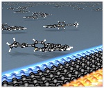
As electronic components are becoming ever smaller, the industry is gradually approaching the limits of what is achievable using the traditional approach with silicon as a semiconductor material. Graphene, the material with a number of "miraculous" properties, is considered a possible replacement. The one atom thin carbon film is ultra-light, extremely flexible and highly conductive. However, in order to be able to use graphene for electronic components such as field effect transistors, the material has to be "transformed" into a semiconductor. This was achieved by Empa scientists some time ago using a newly developed method - in 2010, they presented, for the first time, graphene nanoribbons (GNR) only a few nanometres wide with precisely shaped edges. For this, the ribbons were grown on a metal surface from specifically designed precursor molecules. The narrower the ribbons, the larger their electronic band gap - i.e. the energy range in which no electrons can be located, which is responsible for ensuring that an electronic switch (for example, a transistor) can be turned on and off. The Empa researchers were then also able to "dope" the nanoribbons, i.e. to furnish the ribbons with impurity atoms such as nitrogen at certain points, in order to influence the electronic properties of the graphene ribbons even more.
The perfect blueprint
In the paper now published in Nature, the Empa team led by Roman Fasel reports, together with colleagues from the Max Planck Institute for Polymer Research in Mainz, headed by Klaus Müllen, and from the Technical University of Dresden led by Xinliang Feng, how it managed to synthesise GNR with perfectly zigzagged edges using suitable carbon precursor molecules and a perfected manufacturing process. The zigzags followed a very specific geometry along the longitudinal axis of the ribbons. This is an important step, because researchers can thus give graphene ribbons different properties via the geometry of the ribbons and especially via the structure of their edges.
As with floor tiling, the right tiles - or precursor molecules - for the synthesis on the surface first had to be found for the specific pattern of the zigzag graphene ribbons. Unlike in organic chemistry, which takes the occurrence of by-products into account on the path to achieving a pure substance, everything had to be designed for the surface synthesis of the graphene ribbons so that only a single product was produced. The scientists repeatedly switched back and forth between computer simulations and experiments, in order to design the best possible synthesis. With molecules in a U-shape, which they allowed to grow together to form a snake-like shape, and additional methyl groups, which completed the zigzag edges, the researchers were able to finally create a "blueprint" for GNR with perfect zigzag edges. To check that the zigzag edges were exact down to the atom, the researchers investigated the atomic structure using an atomic force microscope (AFM). In addition, they were able to characterise the electronic states of the zigzag edges using scanning tunnelling spectroscopy (STS).
Page 1 of 2
Share on:


Suggested Items
Warm Windows and Streamlined Skin Patches – IDTechEx Explores Flexible and Printed Electronics
04/26/2024 | IDTechExFlexible and printed electronics can be integrated into cars and homes to create modern aesthetics that are beneficial and easy to use. From luminous car controls to food labels that communicate the quality of food, the uses of this technology are endless and can upgrade many areas of everyday life.
Book Excerpt: The Printed Circuit Assembler’s Guide to... Factory Analytics
04/24/2024 | I-Connect007 Editorial TeamIn our fast-changing, deeply competitive, and margin-tight industry, factory analytics can be the key to unlocking untapped improvements to guarantee a thriving business. On top of that, electronics manufacturers are facing a tremendous burden to do more with less. If you don't already have a copy of this book, what follows is an excerpt from the introduction chapter of 'The Printed Circuit Assembler’s Guide to... Factory Analytics: Unlocking Efficiency Through Data Insights' to whet your appetite.
Listen Up! The Intricacies of PCB Drilling Detailed in New Podcast Episode
04/25/2024 | I-Connect007In episode 5 of the podcast series, On the Line With: Designing for Reality, Nolan Johnson and Matt Stevenson continue down the manufacturing process, this time focusing on the post-lamination drilling process for PCBs. Matt and Nolan delve into the intricacies of the PCB drilling process, highlighting the importance of hole quality, drill parameters, and design optimization to ensure smooth manufacturing. The conversation covers topics such as drill bit sizes, aspect ratios, vias, challenges in drilling, and ways to enhance efficiency in the drilling department.
Elevating PCB Design Engineering With IPC Programs
04/24/2024 | Cory Blaylock, IPCIn a monumental stride for the electronics manufacturing industry, IPC has successfully championed the recognition of the PCB Design Engineer as an official occupation by the U.S. Department of Labor (DOL). This pivotal achievement not only underscores the critical role of PCB design engineers within the technology landscape, but also marks the beginning of a transformative journey toward nurturing a robust, skilled workforce ready to propel our industry into the future.
Winner of The Science Show Rakett 69 Receives Incap Scholarship
04/24/2024 | IncapThe winner of the Rakett 69 science show, Andri Türkson, who stood out as an electronics enthusiast, received a scholarship from Incap Estonia, along with an internship opportunity in Saaremaa.