


 It’s Only Common Sense: Nice Guys Really Can Finish First
 The Right Approach: I Hear the Train A Comin'
 Marcy's Musings: The Growing Industry
Producing Electronics without Semiconductor is Now a Reality
March 29, 2016 | NISTEstimated reading time: 3 minutes
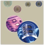
A new study by an international team of researchers, affiliated with UNIST has found a new way to produce electronic devices, such as diodes, logic gates, and sensors without the need of semiconductors.
In their study, published in the current edition of Nano Technology, the team reported that they used metal nanoparticles, coated with charged organic ligands to create versatile electronic circuits, which they have named “chemoelectronic” circuits.
According to the research team, led by Prof. Bartosz Grzybowski (school of Natural Science) of UNIST, this newly developed nanoparticle diodes and devices are durable enough to withstand in salty, aqueous environments and flexible enough to be operated even under significant bending, thereby overcoming the limitations of the present semiconductor technology.
In the study, the team engineered the chemoelectronic devices by coating gold nanoparticles with any of four types of organic molecules, called ligands. Each ligand produces a different, charge-related effect when put in water or a humid environment. One dissolved, releasing a positive ion and leaving the nanoparticle surrounded in negative charge. Another had the opposite effect, making the nanoparticle positive and releasing a negative ion.
This study was jointly conducted by Prof. Bartosz Grzybowski (school of Natural Science) of UNIST, Prof. Yong Yan of the National Center for Nanoscience and Technology in Beijing, Prof. Scott. C Warren of the University of North Carolina at Chapel Hill, and Mr. Patrick Fuller from United States-based company NuMat Technologies.
The following is an interview with Prof. Bartosz Grzybowski (School of Electrical & Computer Engineering):
Q. Wearable devices are a hot topic, these days. As a group leader at IBS Center for Soft Living Matter, could you tell us about the current status of wearable technology and research projects?
A. There is indeed much work on wearable electronics, as well as “implantable” electronics. If I were to choose the leader in this effort, it is John A. Rogers at UIUC. However, at the heart of these technologies are, generally, silicon-based semiconductors and cannot really function when wet. Part of our motivation was to develop a system that can function when wet and is also not toxic — nanoparticles such as Au or Ag meet the non-toxicity condition and so we used them as a basis. Then, the big conceptual thing was how to build electronic components from such metals — they do not have a band-gap like semiconductors, so it might look impossible. But, if one puts these charged groups on the nanoparticles, the counterions around them effectively serve the role of the “p” or “n” carrier in semiconductors. This is quite a radical departure from how we typically think for electronic devices.
Q. Research commercialization plays an important role in the development of wearable technology. Do you and your research group have any strategies for successful commercialization?
A. Our group is in the business of discovering new ideas and I have had several commercial inquiries in the past. However, honestly, I am swamped with science and, at this point, cannot devote my time to commercialization of this stuff. Well, but things might have been different, if “big” players, like Samsung or LG were interested. These guys have the muscles to do things right and do “real” commercialization, unlike academics like us.
Q. What is your standing in the wearable devices industry? In your opinion, how will wearable technology impact our lives?
A. I like the idea of continuous monitoring of the human body, but I also see bunch of ethical problems there, mostly regarding privacy issues. But if we could get better and develop more biocompatible products and devices to monitor patients’ hearts and kidneys, many people will live longer and have better lives. So ultimately I think that should be the future direction for wearable technology.
Share on:


Suggested Items
Samsung Electronics Begins Industry’s First Mass Production of 9th-Gen V-NAND
04/29/2024 | Samsung ElectronicsSamsung Electronics, the world leader in advanced memory technology, today announced that it has begun mass production for its one-terabit (Tb) triple-level cell (TLC) 9th-generation vertical NAND (V-NAND), solidifying its leadership in the NAND flash market.
TSMC Celebrates 30th North America Technology Symposium
04/29/2024 | TSMCTSMC unveiled its newest semiconductor process, advanced packaging, and 3D IC technologies for powering the next generation of AI innovations with silicon leadership at the Company’s 2024 North America Technology Symposium.
QinetiQ Achieves UK’s First Jet-to-Jet Teaming Between Aircraft and Autonomous Drone
04/29/2024 | QinetiQQinetiQ has successfully trialled the UK’s first Crewed-Uncrewed-Teaming demonstration between a crewed aircraft and an autonomous jet drone.
Warm Windows and Streamlined Skin Patches – IDTechEx Explores Flexible and Printed Electronics
04/26/2024 | IDTechExFlexible and printed electronics can be integrated into cars and homes to create modern aesthetics that are beneficial and easy to use. From luminous car controls to food labels that communicate the quality of food, the uses of this technology are endless and can upgrade many areas of everyday life.
iNEMI Packaging Tech Topic Series: Role of EDA in Advanced Semiconductor Packaging
04/26/2024 | iNEMIAdvanced semiconductor packaging with heterogenous integration has made on-package integration of multiple chips a crucial part of finding alternatives to transistor scaling. Historically, EDA tools for front-end and back-end design have evolved separately; however, design complexity and the increased number of die-to-die or die-to-substrate interconnections has led to the need for EDA tools that can support integration of overall design planning, implementation, and system analysis in a single cockpit.