


 It’s Only Common Sense: Nice Guys Really Can Finish First
 The Right Approach: I Hear the Train A Comin'
 Marcy's Musings: The Growing Industry
Terahertz Technology Reaches Industrial Maturity
April 6, 2016 | Fraunhofer IBMTEstimated reading time: 4 minutes
Terahertz is a new technology in which nondestructive testing of components and surfaces is possible. Until now, these devices and, in particular, the sensor heads have been expensive and unwieldy. Researchers at Fraunhofer have now succeeded in making sensor heads more compact and, thus, cheaper, which facilitates their handling considerably. First prototypes are already being used for the production of plastic pipes. They are also very well suited for analyzing coatings of fiber composites. From April 25 to 29, 2016, these new sensor heads are being presented at the Hannover Messe (Hall 2, Stand C16/C22).
More than ten years ago, terahertz technology was the next big thing. Back then there was a lot of talk about ‚nude‘ body scanners. People thought that the devices that were being installed at airports were going to make revealing images of passengers. Moreover, scientists were hoping to develop measurement systems for material testing and inspection of components using terahertz radiation. Despite all these great expectations, the long-awaited breakthrough for terahertz technology did not come about. Compared to the conventional methods currently used for non-destructive testing, such as X-ray or ultrasound, terahertz technology is simply too expensive, unwieldy and overall impractical.
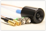
Measuring system with the innovative sensor head
The latest developments of the Fraunhofer Institute for Telecommunication, Heinrich Hertz Institut, HHI in Berlin, could now give terahertz technology a decisive boost. The research team of Thorsten Göbel, who heads the Terahertz Research Group at HHI, has succeeded in developing terahertz devices that for the first time are made from standard and therefore low-cost components and are also relatively easy to handle. At the Hannover Messe, the experts will be presenting a terahertz measuring system with an innovative sensor head, which allows easy testing of various components, such as plastic tubes. The principle employed by Fraunhofer HHI for generating terahertz radiation is based on an optoelectronic method. Using a special semiconductor, laser light pulses are converted into electrical terahertz pulses that are only one billionth of a second long.
The reason for the lack of success of the terahertz technology until now is mainly due to the required properties of the semiconductors being used. These could only be achieved with materials that required an illumination with a wavelength of 800 nanometers. Both the terahertz system‘s laser and optical components are too expensive and not robust enough for industrial use when using this rather exotic wavelength.
Page 1 of 2
Share on:


Suggested Items
Samsung Electronics Begins Industry’s First Mass Production of 9th-Gen V-NAND
04/29/2024 | Samsung ElectronicsSamsung Electronics, the world leader in advanced memory technology, today announced that it has begun mass production for its one-terabit (Tb) triple-level cell (TLC) 9th-generation vertical NAND (V-NAND), solidifying its leadership in the NAND flash market.
TSMC Celebrates 30th North America Technology Symposium
04/29/2024 | TSMCTSMC unveiled its newest semiconductor process, advanced packaging, and 3D IC technologies for powering the next generation of AI innovations with silicon leadership at the Company’s 2024 North America Technology Symposium.
QinetiQ Achieves UK’s First Jet-to-Jet Teaming Between Aircraft and Autonomous Drone
04/29/2024 | QinetiQQinetiQ has successfully trialled the UK’s first Crewed-Uncrewed-Teaming demonstration between a crewed aircraft and an autonomous jet drone.
Warm Windows and Streamlined Skin Patches – IDTechEx Explores Flexible and Printed Electronics
04/26/2024 | IDTechExFlexible and printed electronics can be integrated into cars and homes to create modern aesthetics that are beneficial and easy to use. From luminous car controls to food labels that communicate the quality of food, the uses of this technology are endless and can upgrade many areas of everyday life.
iNEMI Packaging Tech Topic Series: Role of EDA in Advanced Semiconductor Packaging
04/26/2024 | iNEMIAdvanced semiconductor packaging with heterogenous integration has made on-package integration of multiple chips a crucial part of finding alternatives to transistor scaling. Historically, EDA tools for front-end and back-end design have evolved separately; however, design complexity and the increased number of die-to-die or die-to-substrate interconnections has led to the need for EDA tools that can support integration of overall design planning, implementation, and system analysis in a single cockpit.