


 It’s Only Common Sense: Nice Guys Really Can Finish First
 The Right Approach: I Hear the Train A Comin'
 Marcy's Musings: The Growing Industry
Development of Circuit Technology that Resolves Issues with High-Frequency Piezoelectric Resonators
June 20, 2016 | NICTEstimated reading time: 1 minute
In collaboration with the National Institute of Information and Communications Technology (NICT), Associate Professor Hiroyuki Ito and Professor Kazuya Masu, et al., of the Tokyo Institute of Technology, developed a new algorithm and circuit technology allowing high-frequency piezoelectric resonators to be used for phase locked loops (PLL). It was confirmed that these operate with low noise and have an excellent Figure of Merit (FoM) compared to conventional PLLs.
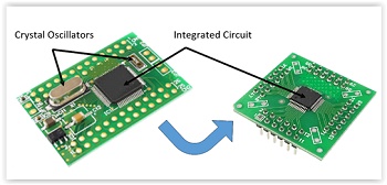
This technology allows high-frequency piezoelectric resonators to be used in place of crystal oscillators which was a problem for realizing compact and low-cost radio modules. This greatly contributes to the creation of compact, low-cost, high-speed radio communication systems for the IoT age. High-frequency piezoelectric resonators are compact, can be integrated, have an excellent Q value, and oscillators that use these have excellent jitter performance. High-frequency piezoelectric resonators had greater issues with resonance frequency variance and temperature dependability compared to crystal resonators. However, these issues were resolved by the development of a PLL that uses a channel adjustment technique, which is a new algorithm.
A prototype was fabricated by a silicon CMOS process with a minimum line width of 65 nm, and a maximum frequency output of approximately 9 GHz was achieved with a phase fluctuation of only 180 femtoseconds. Power consumption was 12.7 mW. This performance is equivalent to a PLL Figure of Merit (FoM) of -244 dB, and it has the world’s top-class performance as a fractional-N PLL. This can contribute to the realization of compact, low-cost, high-speed radio communication systems.
The study results will be announced in local time June 17 in "The 2016 Symposium on VLSI Circuits" to be held in Hawaii from June 14.
Share on:


Suggested Items
Samsung Electronics Begins Industry’s First Mass Production of 9th-Gen V-NAND
04/29/2024 | Samsung ElectronicsSamsung Electronics, the world leader in advanced memory technology, today announced that it has begun mass production for its one-terabit (Tb) triple-level cell (TLC) 9th-generation vertical NAND (V-NAND), solidifying its leadership in the NAND flash market.
TSMC Celebrates 30th North America Technology Symposium
04/29/2024 | TSMCTSMC unveiled its newest semiconductor process, advanced packaging, and 3D IC technologies for powering the next generation of AI innovations with silicon leadership at the Company’s 2024 North America Technology Symposium.
QinetiQ Achieves UK’s First Jet-to-Jet Teaming Between Aircraft and Autonomous Drone
04/29/2024 | QinetiQQinetiQ has successfully trialled the UK’s first Crewed-Uncrewed-Teaming demonstration between a crewed aircraft and an autonomous jet drone.
Warm Windows and Streamlined Skin Patches – IDTechEx Explores Flexible and Printed Electronics
04/26/2024 | IDTechExFlexible and printed electronics can be integrated into cars and homes to create modern aesthetics that are beneficial and easy to use. From luminous car controls to food labels that communicate the quality of food, the uses of this technology are endless and can upgrade many areas of everyday life.
iNEMI Packaging Tech Topic Series: Role of EDA in Advanced Semiconductor Packaging
04/26/2024 | iNEMIAdvanced semiconductor packaging with heterogenous integration has made on-package integration of multiple chips a crucial part of finding alternatives to transistor scaling. Historically, EDA tools for front-end and back-end design have evolved separately; however, design complexity and the increased number of die-to-die or die-to-substrate interconnections has led to the need for EDA tools that can support integration of overall design planning, implementation, and system analysis in a single cockpit.
Copyright © 2024 I-Connect007 | IPC Publishing Group Inc. All rights reserved.
Log in