


 It’s Only Common Sense: Nice Guys Really Can Finish First
 The Right Approach: I Hear the Train A Comin'
 Marcy's Musings: The Growing Industry
Pushing a Single-molecule Switch
July 19, 2016 | University of the Basque CountryEstimated reading time: 3 minutes
An international team of researchers from Donostia International Physics Center, Fritz-Haber Institute of the Max Planck Society, University of Liverpool, and the Polish Academy of Sciences has shown a new way to operate a single-molecule switch by applying an external force.
The combined experimental and theoretical work, published this week in Nature Chemistry, opens a unique capability for studying mechanical activation and processing at the single-molecule level, elementary reactions that are involved in many important biological functions and are crucial in molecular devices.
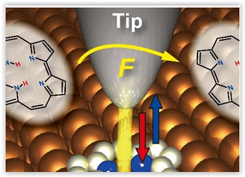
Everybody knows the force that is required to activate a light switch on a wall – a finger is enough. But how much force do you need to apply if the device was dramatically reduced to the "nanoscale world," that is, how much force do you need to operate a "single-molecule switch"? This fundamental question is related not only to basic science but also to potential future applications of molecular devices.
Researchers at Donostia International Physics Center, San Sebastian (Basque Country, Spain), Fritz-Haber Institute of the Max Planck Society, Berlin (Germany), University of Liverpool, (UK) and Polish Academy of Sciences, Warsaw (Poland) have succeeded in activating in a controlled manner a "single-molecule switch" by the force from the atomically-sharp needle of a state-of-the-art scanning probe microscope.
The experimental and theoretical study, reported today in the prestigious journal Nature Chemistry, demonstrates that an intramolecular hydrogen atom transfer can be triggered in a suitable organic molecule adsorbed on a surface by bringing the sharp metallic tip sufficiently close. The reaction, called tautomerization, is important in organic chemistry and molecular biology and also an interesting phenomenon for molecular electronic devices.
The researchers could not only quantify the force needed to operate their tiny switch, a porphycene molecule on a copper surface, but also reveal that the switching can be only induced at a very specific positions of the tip over the molecule, with a spatial resolution of a fraction of a chemical bond length, namely about 0.00000002 millimeter. Furthermore, they demonstrated the significance of the "chemical reactivity" of the tip apex in the force-induced process as the molecule cannot be switched when the apex of the needle is decorated by a single xenon atom – an inert element that lacks the required chemical reactivity.
Takashi Kumagai at FHI-MPG, who conceived this study, constructed the experimental setup in which an oscillating needle of a combined atomic force and scanning tunneling microscope is approached within a few atomic distances to the molecule. The switching showed up as a characteristic feature in the frequency shifts upon approach of the tip and was also confirmed by changes at the atomic-scale images by simultaneously scanning the tip over the molecule. It was measured that the force required was about one nano-Newton, which is a little less than the force needed to break a typical covalent bond between two atoms.
The research team also carried out extensive computer simulations in order to elucidate the atomistic mechanism behind the force-induced switching. The simulations successfully reproduced the experimental results and provided atomistic description on the operation of the single molecule switch. Thomas Frederiksen, Ikerbasque Research Professor at Donostia International Physics Center (DIPC) - UPV/EHU explains that "our calculations revealed that the tautomerization, that is the switching, occurs by a reduction of its energy activation barrier upon approach of a metallic tip. However, the behaviour dramatically changes with a xenon-terminated tip and no tautomerization could be induced because of its inertness and softness."
The researchers emphasize that the studied force-induced reaction involving changes in the reaction pathway resembles an elementary step in catalytic processes. Therefore, their results also provide a novel strategy to gain a deeper atomistic insight into catalytic reactions, leading to a new control of chemistry at the atomic level.
Share on:


Suggested Items
Designer’s Notebook: What Designers Need to Know About Manufacturing, Part 2
04/24/2024 | Vern Solberg -- Column: Designer's NotebookThe printed circuit board (PCB) is the primary base element for providing the interconnect platform for mounting and electrically joining electronic components. When assessing PCB design complexity, first consider the component area and board area ratio. If the surface area for the component interface is restricted, it may justify adopting multilayer or multilayer sequential buildup (SBU) PCB fabrication to enable a more efficient sub-surface circuit interconnect.
Insulectro’s 'Storekeepers' Extend Their Welcome to Technology Village at IPC APEX EXPO
04/03/2024 | InsulectroInsulectro, the largest distributor of materials for use in the manufacture of PCBs and printed electronics, welcomes attendees to its TECHNOLOGY VILLAGE during this year’s IPC APEX EXPO at the Anaheim Convention Center, April 9-11, 2024.
ENNOVI Introduces a New Flexible Circuit Production Process for Low Voltage Connectivity in EV Battery Cell Contacting Systems
04/03/2024 | PRNewswireENNOVI, a mobility electrification solutions partner, introduces a more advanced and sustainable way of producing flexible circuits for low voltage signals in electric vehicle (EV) battery cell contacting systems.
Heavy Copper PCBs: Bridging the Gap Between Design and Fabrication, Part 1
04/01/2024 | Yash Sutariya, Saturn Electronics ServicesThey call me Sparky. This is due to my talent for getting shocked by a variety of voltages and because I cannot seem to keep my hands out of power control cabinets. While I do not have the time to throw the knife switch to the off position, that doesn’t stop me from sticking screwdrivers into the fuse boxes. In all honesty, I’m lucky to be alive. Fortunately, I also have a talent for building high-voltage heavy copper circuit boards. Since this is where I spend most of my time, I can guide you through some potential design for manufacturability (DFM) hazards you may encounter with heavy copper design.
Trouble in Your Tank: Supporting IC Substrates and Advanced Packaging, Part 5
03/19/2024 | Michael Carano -- Column: Trouble in Your TankDirect metallization systems based on conductive graphite or carbon dispersion are quickly gaining acceptance worldwide. Indeed, the environmental and productivity gains one can achieve with these processes are outstanding. In today’s highly competitive and litigious environment, direct metallization reduces costs associated with compliance, waste treatment, and legal issues related to chemical exposure. What makes these processes leaders in the direct metallization space?