


 It’s Only Common Sense: Nice Guys Really Can Finish First
 The Right Approach: I Hear the Train A Comin'
 Marcy's Musings: The Growing Industry
Self-assembling Nano Inks Form Conductive and Transparent Grids During Imprint
July 28, 2016 | INMEstimated reading time: 1 minute
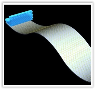
Transparent electronics devices are present in today’s thin film displays, solar cells, and touchscreens. The future will bring flexible versions of such devices. Their production requires printable materials that are transparent and remain highly conductive even when deformed. Researchers at INM – Leibniz Institute for New Materials have combined a new self-assembling nano ink with an imprint process to create flexible conductive grids with a resolution below one micrometer.
To print the grids, an ink of gold nanowires is applied to a substrate. A structured stamp is pressed on the substrate and forces the ink into a pattern. “The nanowires are extremely thin and flexible; they adapt to any pattern of the stamp. During drying, the individual wires self-assemble and form larger, percolating bundles that form the grid,” explains Tobias Kraus from INM. The stamp is removed and the grid is treated in a plasma. “This compresses the bundles into conductive wires and results in a transparent, conductive grid. Depending on the geometry of the stamp, this simple method can shape any nano or microgrid,” says Kraus, head of the program division Structure Formation.
The thickness of the grid can be controlled via the gold concentration. “Only very small quantities of gold are needed to produce a conductive grid, far less than when using inks with spherical gold particles,” says Kraus. This makes the advantages of gold accessible for flexible electronics.
“Our results show self-assembly and imprint can be combined to efficiently produce transparent, conductive materials. We will transfer this insight to other metals in further studies,” says Kraus.
INM conducts research and development to create new materials – for today, tomorrow and beyond. Chemists, physicists, biologists, materials scientists and engineers team up to focus on these essential questions: Which material properties are new, how can they be investigated and how can they be tailored for industrial applications in the future? Four research thrusts determine the current developments at INM: New materials for energy application, new concepts for medical surfaces, new surface materials for tribological systems and nano safety and nano bio. Research at INM is performed in three fields: Nanocomposite Technology, Interface Materials, and Bio Interfaces.
INM – Leibniz Institute for New Materials, situated in Saarbrücken, is an internationally leading centre for materials research. It is an institute of the Leibniz Association and has about 220 employees.
Share on:


Suggested Items
Real Time with... IPC APEX EXPO 2024: Sustainability in the Industry
04/26/2024 | Real Time with...IPC APEX EXPOGuest Editor Henry Crandall and Chris Nash of Indium Corporation discuss the company's 90th anniversary and its focus on sustainability. They focus on the benefits of sustainable materials, their compatibility, and value propositions. The conversation also highlights how Durafuse LT technology's role in reducing reflow temperatures is leading to significant cost and energy savings. Nash also touches on downstream sustainability efforts such as using recycled materials for packaging.
SMC Korea 2024 to Highlight Semiconductor Materials Trends and Innovations on Industry’s Path to $1 Trillion
04/24/2024 | SEMIWith Korea a major consumer of semiconductor materials and advanced materials a key driver of innovation on the industry’s path to $1 trillion, industry leaders and experts will gather at SMC (Strategic Materials Conference) Korea 2024 on May 29 at the Suwon Convention Center in Gyeonggi-do, South Korea to provide insights into the latest materials developments and trends. Registration is open.
Groundbreaking Ceremony Marks the Beginning of a New Era for Newccess Industrial; The Construction of the MINGXIN Building
04/12/2024 | Newccess IndustrialOn a clear and sunny day in March, the groundbreaking ceremony for the MINGXIN Building took place in Shenzhen, China. This moment marked the official commencement of construction for a project that will reshape the semiconductor materials industry.
The Need for a Holistic Global Sustainability Standard
04/10/2024 | Michael Ford, Aegis SoftwareNo one can deny that the resources of our fragile planet are finite. The environment seems like a third party, subject to constant degradation. We’re acutely aware of the effects of pollution on our climate, and despite our “throw-away” culture, recycling and recovery of materials has remained relatively expensive, even as we use more energy just to survive.
iNEMI Publishes Four Roadmap Topics
04/04/2024 | iNEMIThe International Electronics Manufacturing Initiative (iNEMI) announces the availability of the first roadmap topics in the new iNEMI Roadmap format. Printed circuit boards, sustainable electronics, smart manufacturing, and mmWave materials and test are now available online.