


 It’s Only Common Sense: Nice Guys Really Can Finish First
 The Right Approach: I Hear the Train A Comin'
 Marcy's Musings: The Growing Industry
Swapping Substrates Improves Edges of Graphene Nanoribbons
August 4, 2016 | AIP.orgEstimated reading time: 2 minutes
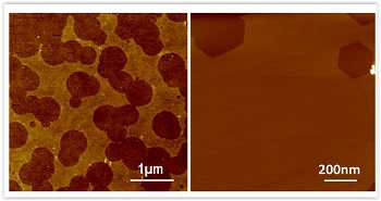
It is now feasible to make a prized material for spintronic devices and semiconductors -- monolayer graphene nanoribbons with zigzag edges.
Miniscule ribbons of graphene are highly sought-after building blocks for semiconductor devices because of their predicted electronic properties. But making these nanostructures has remained a challenge. Now, a team of researchers from China and Japan have devised a new method to make the structures in the lab. Their findings appear in the current issue of Applied Physics Letters, from AIP Publishing.
"Many studies have predicted the properties of graphene nanoribbons with zigzag edges," said Guangyu Zhang, senior author on the study. "But in experiments it's very hard to actually make this material."
Previously, researchers have tried to make graphene nanoribbons by placing sheets of graphene over a layer of silica and using atomic hydrogen to etch strips with zigzag edges, a process known as anisotropic etching. These edges are crucial to modulate the nanoribbon's properties.
But this method only worked well to make ribbons that had two or more graphene layers. Irregularities in silica created by electronic peaks and valleys roughen its surface, so creating precise zigzag edges on graphene monolayers was a challenge. Zhang and his colleagues from the Chinese Academy of Sciences, Beijing Key Laboratory for Nanomaterials and Nanodevices, and the Collaborative Innovation Center of Quantum Matter teamed up with Japanese collaborators from the National Institute for Materials Science to solve the problem.
They replaced the underlying silica with boron nitride, a crystalline material that's chemically sluggish and has a smooth surface devoid of electronic bumps and pits. By using this substrate and the anisotropic etching technique, the group successfully made graphene nanoribbons that were only one-layer thick, and had well-defined zigzag edges.
"This is the first time we have ever seen that graphene on a boron nitride surface can be fabricated in such a controllable way," Zhang explained.
The zigzag-edged nanoribbons showed high electron mobility in the range of 2000 cm2/Vs even at widths of less than 10nm -- the highest value ever reported for these structures -- and created clean, narrow energy band gaps, which makes them promising materials for spintronic and nano-electronic devices.
"When you decrease the width of the nanoribbons, the mobility decreases drastically because of edge defects," said Zhang. "Using standard lithography fabrication techniques, studies have seen mobility of 100 cm2/Vs or even lower, but our material still exceeds 2000 cm2/Vs even at the sub-10 nanometer scale, demonstrating that these nanoribbons are of very high quality."
In future studies, extending this method to other kinds of substrates could enable the quick large scale processing of monolayers of graphene to make high-quality nanoribbons with zigzag edges.
Share on:


Suggested Items
Latest Test and Inspection Solutions from GOEPEL electronic at SMTconnect 2024
04/29/2024 | GOEPEL electronicGOEPEL electronic will be demonstrating automated test and inspection equipment at SMTconnect, taking place in Nuremberg from June 11 to 13, 2024.
SCHWEIZER Confirms Group Figures and Outlook for 2024
04/29/2024 | SCHWEIZERSCHWEIZER announces the publication of the annual report for 2023 and confirms the preliminary figures. The SCHWEIZER-Group (according to IFRS) generated sales of EUR 139.4 million in 2023 (previous year: EUR 131.0 million).
Arlon Electronic Materials Awarded Requalification to IPC-4101 QPL for All Polyimide Specification Sheets
04/29/2024 | IPCIPC's Validation Services Program has awarded Arlon Electronic Materials Division, an electronics material manufacturing company headquartered in Rancho Cucamonga, Calif., an IPC-4101 Qualified Products Listing (QPL) requalification for the third time.
Warm Windows and Streamlined Skin Patches – IDTechEx Explores Flexible and Printed Electronics
04/26/2024 | IDTechExFlexible and printed electronics can be integrated into cars and homes to create modern aesthetics that are beneficial and easy to use. From luminous car controls to food labels that communicate the quality of food, the uses of this technology are endless and can upgrade many areas of everyday life.
Book Excerpt: The Printed Circuit Assembler’s Guide to... Factory Analytics
04/24/2024 | I-Connect007 Editorial TeamIn our fast-changing, deeply competitive, and margin-tight industry, factory analytics can be the key to unlocking untapped improvements to guarantee a thriving business. On top of that, electronics manufacturers are facing a tremendous burden to do more with less. If you don't already have a copy of this book, what follows is an excerpt from the introduction chapter of 'The Printed Circuit Assembler’s Guide to... Factory Analytics: Unlocking Efficiency Through Data Insights' to whet your appetite.