


 It’s Only Common Sense: Nice Guys Really Can Finish First
 The Right Approach: I Hear the Train A Comin'
 Marcy's Musings: The Growing Industry
X-ray Optics on a Chip
August 18, 2016 | International Union of CrystallographyEstimated reading time: 1 minute
Waveguides are widely used for filtering, confining, guiding, coupling or splitting beams of visible light. However, creating waveguides that could do the same for X-rays has posed tremendous challenges in fabrication, so they are still only in an early stage of development.
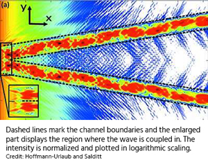
In the latest issue of Acta Crystallographica Section A: Foundations and Advances , Sarah Hoffmann-Urlaub and Tim Salditt report the fabrication and testing of a millimetre-sized chip capable of splitting a beam of X-rays. Fork-shaped channels that are only a few tens of nanometres wide and deep are transferred into a silicon wafer using electron-beam lithography and reactive ion etching then enclosed by bonding a second silicon wafer on top. The results of simulations of how the 'parent' beam is split into two 'daughter' beams on passing through the chip were backed up by experimental measurements at the European Synchrotron Radiation Facility, showing that the incident beam is efficiently transported through the chip, neatly split and guided to exits that have precisely controlled (and tunable) spacings. After the daughter beams leave the chip, they interfere, leading to a pattern of vertical stripes just like the pattern obtained from a classical Young's double-slit interference experiment. Interestingly, on close inspection there are fork-like structures within the stripes that originate from discontinuities in the phase of the recombined beam, forming striking features known as phase vortices. Furthermore, from those interference patterns the intensity distribution in the exit plane of the channels is reconstructed, which is found to be in very good agreement to the actual channel design.
This study complements earlier work on two-dimensionally confined channels in silicon in straight and tapered geometries, and paves the way to realizing `X-ray optics on a chip'. Illumination of samples by the two beams could provide some interesting advantages for coherent imaging and opens up the possibility of a new form of nano-interferometer. The authors envisage future development of their beamsplitter to create several daughter beams from the same parent beam, which would allow a single object to be imaged simultaneously by several beams, each from a different direction.
Share on:


Suggested Items
Merlin Flex invests in New Schmoll Direct Imaging System
04/30/2024 | Merlin Flex LtdMerlin Flex has fully installed and commissioned its 2nd Schmoll MDI Direct Imaging system. This new machine includes a twin bed, 4 head system which enhances Merlin Flex’s direct imaging capability for its 1.4M long flexible circuits.
Inkjet Solder Mask ‘Has Arrived’
04/10/2024 | Pete Starkey, I-Connect007I was delighted to be invited to attend an interactive webinar entitled “Solder Mask Coating Made Easy with Additive Manufacturing,” hosted by SUSS MicroTec Netherlands in Eindhoven. The webinar was introduced and moderated by André Bodegom, managing director at Adeon Technologies, and the speakers were Mariana Van Dam, senior product manager PCB imaging solutions at AGFA in Belgium; Ashley Steers, sales manager at Electra Polymers in the UK; and Dr. Luca Gautero, product manager at SUSS MicroTec Netherlands.
NetVia Group Acquires Direct Imaging from Mivatek
04/09/2024 | Miva TechnologiesMiva Technologies is pleased to announce NetVia Group, Irving, TX has acquired a new Miva 2400NG Dual Tray Direct Imaging System with 30-micron capabilities for inner, outer and soldermask imaging.
Teledyne to Acquire Adimec
02/13/2024 | TeledyneTeledyne Technologies Incorporated announced that it has entered into an agreement to acquire Adimec Holding B.V. and its subsidiaries.
Real Time with... productronica 2023: MivaTek Global Advances Technology With High-res Imaging System
12/08/2023 | Real Time with...productronicaMivaTek's Brendan Hogan talks about how the company employs Digitally Adaptive Rasterization Technology (DART) in their high-res imaging equipment. He also shares how the blurred line between semiconductors and microelectronics is driving broader application of the imaging process.