


 It’s Only Common Sense: Nice Guys Really Can Finish First
 The Right Approach: I Hear the Train A Comin'
 Marcy's Musings: The Growing Industry
Tiny Lasers that Opens New Era for Light-based Computing
August 22, 2016 | HKUSTEstimated reading time: 1 minute
Researchers at The Hong Kong University of Science and Technology (HKUST) have fabricated microscopically-small lasers directly on silicon, enabling the future-generation microprocessors to run faster and less power-hungry – a significant step towards light-based computing.
The innovation, made by Prof Kei-may Lau, Fang Professor of Engineering and Chair Professor of the Department of Electronic and Computer Engineering, in collaboration with the University of California, Santa Barbara; Sandia National Laboratories and Harvard University, marks a major breakthrough for the semiconductor industry and well beyond.
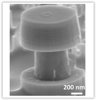
Silicon forms the basis of everything from solar cells to the integrated circuits at the heart of our modern electronic gadgets. However, the crystal lattice of silicon and of typical laser materials could not match up, making it impossible to integrate the two materials until now, when Prof Lau’s group managed to integrate subwavelength cavities — the essential building blocks of their tiny lasers — onto silicon, allowing them to create and demonstrate high-density on-chip light-emitting elements. The finding was recently published as the cover story on Applied Physics Letters.
“These whispering gallery mode lasers are extremely attractive light source for on-chip optical communications, data processing and chemical sensing applications,” Prof Lau said. “Putting lasers on microprocessors boosts their capabilities and allows them to run at much lower powers – a big step towards photonics and electronics integration on the silicon platform and a key solution to the next-generation green information technology.”
For years, photonics had been the most energy-efficient and cost-effective method to transmit large volumes of data over long distances, now with these new silicon-based integrated lasers, photonics may be able to use for short-distance data transmission as well, which is set to greatly enhance the speed of data communication.
In fabricating these “whispering gallery mode lasers”, Prof Lau’s team etched nano-patterns directly onto the silicon, so as to confine the defects of its crystal lattices while ensuring the necessary quantum confinement of electrons within quantum dots grown on this template. Her team then use optical pumping – a process that uses light to raise or “pump” electrons from a lower energy level to a higher one, to demonstrate that the devices they created were able to operate as lasers.
These tiny lasers measure only 1 micron in diameter, and are 1,000 times shorter in length and 1 million times smaller in area than those currently used.
Share on:


Suggested Items
Indium Corporation Expert to Present on Pb-Free Solder for Die-Attach in Discrete Power Applications
04/30/2024 | Indium CorporationIndium Corporation Product Manager – Semiconductor Dean Payne will present at the Advanced Packaging for Power Electronics conference, hosted by IMAPS, held May 8-9 in Woburn, Massachusetts, USA.
Real Time with... IPC APEX EXPO 2024: Adhesive Materials and Equipment Update with Dymax
05/01/2024 | Real Time with...IPC APEX EXPOVirginia Hogan, global business development manager at Dymax, discusses adhesive materials, dispensing and curing equipment, a new, high-reliability conformal coating, and various materials and dispensing methods.
Real Time with... IPC APEX EXPO 2024: Sustainability in the Industry
04/26/2024 | Real Time with...IPC APEX EXPOGuest Editor Henry Crandall and Chris Nash of Indium Corporation discuss the company's 90th anniversary and its focus on sustainability. They focus on the benefits of sustainable materials, their compatibility, and value propositions. The conversation also highlights how Durafuse LT technology's role in reducing reflow temperatures is leading to significant cost and energy savings. Nash also touches on downstream sustainability efforts such as using recycled materials for packaging.
SMC Korea 2024 to Highlight Semiconductor Materials Trends and Innovations on Industry’s Path to $1 Trillion
04/24/2024 | SEMIWith Korea a major consumer of semiconductor materials and advanced materials a key driver of innovation on the industry’s path to $1 trillion, industry leaders and experts will gather at SMC (Strategic Materials Conference) Korea 2024 on May 29 at the Suwon Convention Center in Gyeonggi-do, South Korea to provide insights into the latest materials developments and trends. Registration is open.
Groundbreaking Ceremony Marks the Beginning of a New Era for Newccess Industrial; The Construction of the MINGXIN Building
04/12/2024 | Newccess IndustrialOn a clear and sunny day in March, the groundbreaking ceremony for the MINGXIN Building took place in Shenzhen, China. This moment marked the official commencement of construction for a project that will reshape the semiconductor materials industry.