


 It’s Only Common Sense: Nice Guys Really Can Finish First
 The Right Approach: I Hear the Train A Comin'
 Marcy's Musings: The Growing Industry
New Theory Could Lead to New Generation of Energy Friendly Optoelectronics
August 22, 2016 | Queen’s University BelfastEstimated reading time: 1 minute
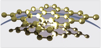
Researchers at Queen’s University Belfast and ETH Zurich, Switzerland, have created a new theoretical framework which could help physicists and device engineers design better optoelectronics, leading to less heat generation and power consumption in electronic devices which source, detect, and control light.
Speaking about the research, which enables scientists and engineers to quantify how transparent a 2D material is to an electrostatic field, Dr Elton Santos from the Atomistic Simulation Research Centre at Queen’s, said: “In our paper we have developed a theoretical framework that predicts and quantifies the degree of ‘transparency’ up to the limit of one-atom-thick, 2D materials, to an electrostatic field.
“Imagine we can change the transparency of a material just using an electric bias, e.g. get darker or brighter at will. What kind of implications would this have, for instance, in mobile phone technologies? This was the first question we asked ourselves. We realised that this would allow the microscopic control over the distribution of charged carriers in a bulk semiconductor (e.g. traditional Si microchips) in a nonlinear manner. This will help physicists and device engineers to design better quantum capacitors, an array of subatomic power storage components capable to keep high energy densities, for instance, in batteries, and vertical transistors, leading to next-generation optoelectronics with lower power consumption and dissipation of heat (cold devices), and better performance. In other words, smarter smart phones.”
Explaining how the theory could have important implications for future work in the area, Dr Santos added: “Our current model simply considers an interface formed between a layer of 2D material and a bulk semiconductor. In principle, our approach can be readily extended to a stack of multiple 2D materials, or namely, van der Waals heterostructures recently fabricated. This will allow us to design and predict the behaviour of these cutting-edge devices in prior to actual fabrication, which will significantly facilitate developments for a variety of applications. We will have an in silico search for the right combination of different 2D crystals while reducing the need for expensive lab work and test trials.”
Share on:


Suggested Items
Real Time with… IPC APEX EXPO 2024: Ventec Discusses New Pro-bond Family of Advanced Products
05/01/2024 | Real Time with...IPC APEX EXPOChris Hanson, Ventec's Global Head of IMS Technology, outlines the launch of four pro-bond formulas that deliver an outstanding combination of low dissipation factor (Df) with a dielectric constant (Dk) range to maximize the design window for critical PCB parameters. As Chris points out, Pro-bond is designed for low-loss, high-speed applications, while thermal-bond dissipates heat from a component through the board to a heat sink.
IPC's Vision for Empowering PCB Design Engineers
04/30/2024 | Robert Erickson, IPCAs architects of innovation, printed circuit board designers are tasked with translating increasingly complex concepts into tangible designs that power our modern world. IPC provides the necessary community, standards framework, and education to prepare these pioneers as they explore the boundaries of what’s possible, equipping engineers with the knowledge, skills, and resources required to thrive in an increasingly dynamic field.
iNEMI Packaging Tech Topic Series: Role of EDA in Advanced Semiconductor Packaging
04/26/2024 | iNEMIAdvanced semiconductor packaging with heterogenous integration has made on-package integration of multiple chips a crucial part of finding alternatives to transistor scaling. Historically, EDA tools for front-end and back-end design have evolved separately; however, design complexity and the increased number of die-to-die or die-to-substrate interconnections has led to the need for EDA tools that can support integration of overall design planning, implementation, and system analysis in a single cockpit.
Cadence, TSMC Collaborate on Wide-Ranging Innovations to Transform System and Semiconductor Design
04/25/2024 | Cadence Design SystemsCadence Design Systems, Inc. and TSMC have extended their longstanding collaboration by announcing a broad range of innovative technology advancements to accelerate design, including developments ranging from 3D-IC and advanced process nodes to design IP and photonics.
Ansys, TSMC Enable a Multiphysics Platform for Optics and Photonics, Addressing Needs of AI, HPC Silicon Systems
04/25/2024 | PRNewswireAnsys announced a collaboration with TSMC on multiphysics software for TSMC's Compact Universal Photonic Engines (COUPE). COUPE is a cutting-edge Silicon Photonics (SiPh) integration system and Co-Packaged Optics platform that mitigates coupling loss while significantly accelerating chip-to-chip and machine-to-machine communication.