


 The Chemical Connection: Reducing Etch System Water Usage, Part 2
 It’s Only Common Sense: Nice Guys Really Can Finish First
 The Right Approach: I Hear the Train A Comin'
New Technique Integrates Graphene, GO and rGO onto Silicon Chips at Room Temperature
September 14, 2016 | North Carolina State UniversityEstimated reading time: 1 minute
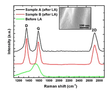
Materials researchers at North Carolina State University have developed a technique that allows them to integrate graphene, graphene oxide (GO) and reduced graphene oxide (rGO) onto silicon substrates at room temperature by using nanosecond pulsed laser annealing. The advance raises the possibility of creating new electronic devices, and the researchers are already planning to use the technique to create smart biomedical sensors.
In the new technique, researchers start with a silicon substrate. They top that with a layer of single-crystal titanium nitride, using domain matching epitaxy to ensure the crystalline structure of the titanium nitride is aligned with the structure of the silicon. Researchers then place a layer of copper-carbon (Cu-2.0atomic percent C) alloy on top of the titanium nitride, again using domain matching epitaxy. Finally, the researchers melt the surface of the alloy with nanosecond laser pulses, which pulls carbon to the surface.
If the process is done in a vacuum, the carbon forms on the surface as graphene; if it is done in oxygen, it forms GO; and if done in a humid atmosphere followed by a vacuum, it forms as rGO. In all three cases, the carbon’s crystalline structure is aligned with the underlying copper-carbon alloy.
“We can control whether the carbon forms one or two monolayers on the surface of the material by manipulating the intensity of the laser and the depth of the melting,” says Jay Narayan, the John C. Fan Distinguished Chair Professor of Materials Science and Engineering at NC State and senior author of a paper describing the work.
“The process can easily be scaled up,” Narayan says. “We’ve made wafers that are two inches square, and could easily make them much larger, using lasers with higher Hertz. And this is all done at room temperature, which drives down the cost.”
Graphene is an excellent conductor, but it cannot be used as a semiconductor. However, rGO is a semiconductor material, which can be used to make electronic devices such as integrated smart sensors and optic-electronic devices.
“We have already patented the technique and are planning to use it to develop smart biomedical sensors integrated with computer chips,” Narayan says.
Share on:


Suggested Items
The Chemical Connection: Reducing Etch System Water Usage, Part 2
05/02/2024 | Don Ball -- Column: The Chemical ConnectionIn my last column, I reviewed some relatively simple ways to reduce water usage in existing etch systems: cutting down cooling coil water flow, adding chillers to replace plant water for cooling, lowering flow rate nozzles for rinses, etc. This month, I’ll continue with more ways to control water usage in your etcher. Most of these are not easily retrofittable to existing equipment but should be given serious consideration when new equipment is contemplated. With the right combination of add-ons, it is possible to bring the amount of water used in an etch system to almost zero.
Designer’s Notebook: What Designers Need to Know About Manufacturing, Part 2
04/24/2024 | Vern Solberg -- Column: Designer's NotebookThe printed circuit board (PCB) is the primary base element for providing the interconnect platform for mounting and electrically joining electronic components. When assessing PCB design complexity, first consider the component area and board area ratio. If the surface area for the component interface is restricted, it may justify adopting multilayer or multilayer sequential buildup (SBU) PCB fabrication to enable a more efficient sub-surface circuit interconnect.
Insulectro’s 'Storekeepers' Extend Their Welcome to Technology Village at IPC APEX EXPO
04/03/2024 | InsulectroInsulectro, the largest distributor of materials for use in the manufacture of PCBs and printed electronics, welcomes attendees to its TECHNOLOGY VILLAGE during this year’s IPC APEX EXPO at the Anaheim Convention Center, April 9-11, 2024.
ENNOVI Introduces a New Flexible Circuit Production Process for Low Voltage Connectivity in EV Battery Cell Contacting Systems
04/03/2024 | PRNewswireENNOVI, a mobility electrification solutions partner, introduces a more advanced and sustainable way of producing flexible circuits for low voltage signals in electric vehicle (EV) battery cell contacting systems.
Heavy Copper PCBs: Bridging the Gap Between Design and Fabrication, Part 1
04/01/2024 | Yash Sutariya, Saturn Electronics ServicesThey call me Sparky. This is due to my talent for getting shocked by a variety of voltages and because I cannot seem to keep my hands out of power control cabinets. While I do not have the time to throw the knife switch to the off position, that doesn’t stop me from sticking screwdrivers into the fuse boxes. In all honesty, I’m lucky to be alive. Fortunately, I also have a talent for building high-voltage heavy copper circuit boards. Since this is where I spend most of my time, I can guide you through some potential design for manufacturability (DFM) hazards you may encounter with heavy copper design.