


 The Chemical Connection: Reducing Etch System Water Usage, Part 2
 It’s Only Common Sense: Nice Guys Really Can Finish First
 The Right Approach: I Hear the Train A Comin'
Nanoscale Tetrapods Could Provide Early Warning of a Material’s Failure
September 20, 2016 | LBLEstimated reading time: 3 minutes
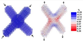
Light-emitting, four-armed nanocrystals could someday form the basis of an early warning system in structural materials by revealing microscopic cracks that portend failure, thanks to recent research by scientists from the U.S. Department of Energy’s Lawrence Berkeley National Laboratory (Berkeley Lab) and UC Berkeley.
The researchers embedded tetrapod-shaped quantum dots, which are nanosized semiconducting particles, in a polymer film. The tetrapods’ cores emit fluorescent light when their arms are twisted or bent out of shape. This indicates the polymer is undergoing a degree of tensile or compressive strain, from which stress over sub-micron-scale regions of the material can be detected. Such stress can cause nanoscale cracks to develop into macroscopic failure. Initial tests show the tetrapods can cycle more than 20 times without losing their ability to sense stress, and they don’t degrade the strength of the polymer in which they’re matrixed.
So far the scientists have tested their approach in the lab, but in practice, all that would be needed to detect the tetrapods’ fluorescent warning is an off-the-shelf, portable spectrometer. A person could point a spectrometer at a steel beam, airplane wing, or any material that has the tetrapods embedded inside, and the spectrometer could potentially detect incipient cracks that are only 100 nanometers long.
“This is the length scale at which cracks develop, which is when you want to catch them, well before the material fails,” says Shilpa Raja, who conducted the research while she was an affiliate in Berkeley Lab’s Materials Sciences Division and a PhD student at UC Berkeley. Raja is now a postdoctoral scholar at Stanford University. Robert Ritchie and Paul Alivisatos, also of the Materials Sciences Division and UC Berkeley, are the co-corresponding authors of a paper on this research published online in the journal Nano Letters (2016, vol. 16, issue 8, pgs. 5060-5067).
“Our approach could also be a big step toward self-healing smart materials. The tetrapods could be coupled with nanosized repair particles to form a material that senses local stress and then repairs itself,” adds Raja.
In addition to materials applications, the tetrapods could potentially be used to detect the presence of cancerous cells in tissue samples because cancerous cells have different mechanical properties than healthy cells, such as an increased stiffness.
To develop the technique, the scientists started with a polymer widely used in airframes and other structures. They mixed tetrapod nanocrystals into the polymer and cast slabs of the mixture in petri dishes. The slabs were then mounted in a tensile tester and exposed to a laser. This allowed the researchers to simultaneously measure the slab’s fluorescence and mechanical stress.
“This is a low-cost fabrication technique, and it resulted in the best optomechanical agreement between fluorescence and mechanical tests sensed by a nanocrystal in a film,” says Raja.
Raja says the tetrapods’ shape makes them very sensitive to stress. Their four arms act as antennae that take stress from their immediate environment, amplify the stress, and transfer it to the core. The color of light emitted by the core indicates the degree of stress (and strain) felt by the arms.
Their approach promises to be a big improvement over current ways to detect nanoscale stress in materials, particularly in the field. This can be done in the lab with techniques like atomic force microscopy and nano-indentation techniques, but these require a very controlled environment. Over the past five years, scientists have developed ways to matrix other stress-sensing nanoparticles into materials, but these methods have a very low signal-to-noise ratio and don’t use visible light detection. In addition, some of these approaches degrade the mechanical properties of the material they’re embedded in, or they can’t cycle back and forth, meaning they can only give a warning signal once.
Atom-scale computer simulations of the tetrapod were conducted at the National Energy Research Scientific Computing Center (NERSC). And electron tomography of the tetrapods under stress was conducted at the Molecular Foundry. Both facilities are DOE Office of Science User Facilities located at Berkeley Lab.
The research was funded in part by the Department of Energy’s Office of Science.
Share on:


Suggested Items
LQDX Divests Aluminum Soldering Business - Mina™ - to Taiyo America Inc.
05/02/2024 | PRNewswireLQDX, formerly known as Averatek Corp., developer of high-performance materials for advanced semiconductor manufacturing, today announced that it has divested its aluminum soldering business – known as MinaTM – to Taiyo America Inc., a global market leader in advanced electronic materials.
Indium Corporation Expert to Present on Pb-Free Solder for Die-Attach in Discrete Power Applications
04/30/2024 | Indium CorporationIndium Corporation Product Manager – Semiconductor Dean Payne will present at the Advanced Packaging for Power Electronics conference, hosted by IMAPS, held May 8-9 in Woburn, Massachusetts, USA.
Real Time with... IPC APEX EXPO 2024: Adhesive Materials and Equipment Update with Dymax
05/01/2024 | Real Time with...IPC APEX EXPOVirginia Hogan, global business development manager at Dymax, discusses adhesive materials, dispensing and curing equipment, a new, high-reliability conformal coating, and various materials and dispensing methods.
Real Time with... IPC APEX EXPO 2024: Sustainability in the Industry
04/26/2024 | Real Time with...IPC APEX EXPOGuest Editor Henry Crandall and Chris Nash of Indium Corporation discuss the company's 90th anniversary and its focus on sustainability. They focus on the benefits of sustainable materials, their compatibility, and value propositions. The conversation also highlights how Durafuse LT technology's role in reducing reflow temperatures is leading to significant cost and energy savings. Nash also touches on downstream sustainability efforts such as using recycled materials for packaging.
SMC Korea 2024 to Highlight Semiconductor Materials Trends and Innovations on Industry’s Path to $1 Trillion
04/24/2024 | SEMIWith Korea a major consumer of semiconductor materials and advanced materials a key driver of innovation on the industry’s path to $1 trillion, industry leaders and experts will gather at SMC (Strategic Materials Conference) Korea 2024 on May 29 at the Suwon Convention Center in Gyeonggi-do, South Korea to provide insights into the latest materials developments and trends. Registration is open.