


 Marcy's Musings: The Growing Industry
 It’s Only Common Sense: Here’s What To Do After IPC APEX EXPO 2024
 Dan’s Biz Bookshelf: Seeing the How
Livermore Scientists Purify Copper Nanowires
September 26, 2016 | Lawrence Livermore National LaboratoryEstimated reading time: 2 minutes
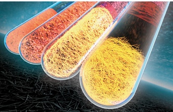
Cell phones and Apple watches could last a little longer due to a new method to create copper nanowires.
A team of Lawrence Livermore National Laboratory (LLNL) scientists have created a new method to purify copper nanowires with a near-100 percent yield. These nanowires are often used in nanoelectronic applications.
The research, which appears in the online edition of Chemical Communications (link is external)and on the cover of the hardcopy issue, shows how the method can yield large quantities of long, uniform, high-purity copper nanowires. High-purity copper nanowires meet the requirements of nanoelectronic applications as well as provide an avenue for purifying industrial-scale synthesis of copper nanowires, a key step for commercialization and application.
Metal nanowires (NWs) hold promise for commercial applications such as flexible displays, solar cells, catalysts and heat dissipators.
The most common approach to create nanowires not only yield nanowires but also other low-aspect ratio shapes such as nanoparticles (NPs) and nanorods. These undesired byproducts are almost always produced due to difficulties in controlling the non-instantaneous nucleation of the seed particles as well as seed types, which causes the particles to grow in multiple pathways.
"We created the purest form of copper nanowires with no byproducts that would affect the shape and purity of the nanowires," said LLNL's Fang Qian, lead author of the paper.
The team demonstrated that copper nanowires, synthesized at a liter-scale, can be purified to near 100 percent yield from their nanoparticle side-products with a few simple steps.
Functional nanomaterials are notoriously difficult to produce in large volumes with highly controlled composition, shapes and sizes. This difficulty has limited adoption of nanomaterials in many manufacturing technologies.
"This work is important because it enables production of large quantities of copper nanomaterials with a very facile and elegant approach to rapidly separate nanowires from nanoparticles with extremely high efficiency," said Eric Duoss, a principal investigator on the project. "We envision employing these purified nanomaterials for a wide variety of novel fabrication approaches, including additive manufacturing."
The key to success is the use of a hydrophobic surfactant in aqueous solution, together with an immiscible water organic solvent system to create a hydrophobic-distinct interface, allowing nanowires to crossover spontaneously due to their different crystal structure and total surface area from those of nanoparticles.
"The principles developed from this particular case of copper nanowires may be applied to a variety of nanowire applications," Qian said. "This purification method will open up new possibilities in producing high quality nanomaterials with low cost and in large quantities."
Other Livermore researchers include: Pui Ching Lan, Tammy Olson, Cheng Zhu and Christopher Spadaccini.
"We also are developing high surface area foams as well as printable inks for additive manufacturing processes, such as direct-ink writing using the NWs," said LLNL's Yong Han, a corresponding author of the paper.
Share on:


Suggested Items
Insulectro’s 'Storekeepers' Extend Their Welcome to Technology Village at IPC APEX EXPO
04/03/2024 | InsulectroInsulectro, the largest distributor of materials for use in the manufacture of PCBs and printed electronics, welcomes attendees to its TECHNOLOGY VILLAGE during this year’s IPC APEX EXPO at the Anaheim Convention Center, April 9-11, 2024.
ENNOVI Introduces a New Flexible Circuit Production Process for Low Voltage Connectivity in EV Battery Cell Contacting Systems
04/03/2024 | PRNewswireENNOVI, a mobility electrification solutions partner, introduces a more advanced and sustainable way of producing flexible circuits for low voltage signals in electric vehicle (EV) battery cell contacting systems.
Heavy Copper PCBs: Bridging the Gap Between Design and Fabrication, Part 1
04/01/2024 | Yash Sutariya, Saturn Electronics ServicesThey call me Sparky. This is due to my talent for getting shocked by a variety of voltages and because I cannot seem to keep my hands out of power control cabinets. While I do not have the time to throw the knife switch to the off position, that doesn’t stop me from sticking screwdrivers into the fuse boxes. In all honesty, I’m lucky to be alive. Fortunately, I also have a talent for building high-voltage heavy copper circuit boards. Since this is where I spend most of my time, I can guide you through some potential design for manufacturability (DFM) hazards you may encounter with heavy copper design.
Trouble in Your Tank: Supporting IC Substrates and Advanced Packaging, Part 5
03/19/2024 | Michael Carano -- Column: Trouble in Your TankDirect metallization systems based on conductive graphite or carbon dispersion are quickly gaining acceptance worldwide. Indeed, the environmental and productivity gains one can achieve with these processes are outstanding. In today’s highly competitive and litigious environment, direct metallization reduces costs associated with compliance, waste treatment, and legal issues related to chemical exposure. What makes these processes leaders in the direct metallization space?
AT&S Shines with Purest Copper on World Recycling Day
03/18/2024 | AT&SThe Styrian microelectronics specialist AT&S is taking World Recycling Day as an opportunity to review the progress that has been made in recent months at its sites around the world in terms of the efficient use of resources: