


 Marcy's Musings: The Growing Industry
 It’s Only Common Sense: Here’s What To Do After IPC APEX EXPO 2024
 Dan’s Biz Bookshelf: Seeing the How
Record for Perovskite/CIGS Tandem Solar Module
September 27, 2016 | KITEstimated reading time: 2 minutes
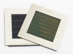
Thin-film technologies can dramatically reduce the cost of next-generation solar modules. Whereas their production cost is low, it is in particular the combination of complementary absorber materials in a tandem solar module that increases the power conversion efficiency. At the PSCO international conference in Genova, researchers from KIT, ZSW, and the Belgian research institute imec present a perovskite/CIGS tandem thin-film solar module that achieves 17.8 percent in efficiency, surpassing for the first time the efficiency of separate perovskite and CIGS solar modules.
“Our prototype demonstrates that scalable perovskite/CIGS solar modules can drastically surpass the efficiency of a separate solar module made of these materials,” emphasizes Dr. Ulrich W. Paetzold of KIT. His newly established young investigators group at KIT’s Institute of Microstructure Technology and Institute of Light Technology investigates and optimizes light trapping and energy efficiency in these tandem solar modules.
Professor Michael Powalla, head of the Thin-film Photovoltaics Division at KIT as well as member of the board and head of the Photovoltaics Division at ZSW, points out: “The novel stacked module is an elegant way of making optimum use of a large part of the solar spectrum by combining the advantages of two highly innovative thin-film technologies.” Whereas the semitransparent upper perovskite solar module efficiently absorbs the high-energy portion of the solar spectrum, the lower CIGS (Copper Indium Gallium Selenide) layer converts the infrared parts. In total, the prototype achieves an energy conversion efficiency of 17.8 percent. For comparison, the current world record for perovskite modules on this scale is at 15.3 percent, and the reference CIGS solar module has an efficiency of 15.7 percent.
Besides, the stacked module implements a fully scalable device concept that matches industrial needs. Both, the perovskite top module and the CIGS bottom module feature an aperture area of 3.67 square centimeter and a monolithic interconnection scheme, using 4 and 7 module cell stripes respectively. The area losses are less than 8 percent for both technologies and the interconnection can be laser-processed, allowing industrial scaling to stacked modules of several square meters. All previous reports on this technology have been limited to very small scale solar cells. The presented achievement takes the technology to large area and scalable solar module architecture which show remarkable power conversion efficiencies.
Tom Aernouts, team leader head of thin-film PV research at imec commented: “This result was made possible by combining the complementary world-leading expertise of the three partners in a very fruitful collaboration.” Whereas the Belgian research institute imec is a leader in the manufacture of semitransparent perovskite solar modules, ZSW is a pioneer in the development and scaling of CIGS-based solar cells and modules and holds the efficiency world record of 22.6 percent for CIGS thin-film solar cells which are the basic elements for interconnected solar modules. The Helmholtz Young Investigators Group at KIT, headed by Dr. Ulrich W. Paetzold, studies the optics in these components and develops new nanophotonic materials for improved light harvesting.
Share on:


Suggested Items
Insulectro’s 'Storekeepers' Extend Their Welcome to Technology Village at IPC APEX EXPO
04/03/2024 | InsulectroInsulectro, the largest distributor of materials for use in the manufacture of PCBs and printed electronics, welcomes attendees to its TECHNOLOGY VILLAGE during this year’s IPC APEX EXPO at the Anaheim Convention Center, April 9-11, 2024.
ENNOVI Introduces a New Flexible Circuit Production Process for Low Voltage Connectivity in EV Battery Cell Contacting Systems
04/03/2024 | PRNewswireENNOVI, a mobility electrification solutions partner, introduces a more advanced and sustainable way of producing flexible circuits for low voltage signals in electric vehicle (EV) battery cell contacting systems.
Heavy Copper PCBs: Bridging the Gap Between Design and Fabrication, Part 1
04/01/2024 | Yash Sutariya, Saturn Electronics ServicesThey call me Sparky. This is due to my talent for getting shocked by a variety of voltages and because I cannot seem to keep my hands out of power control cabinets. While I do not have the time to throw the knife switch to the off position, that doesn’t stop me from sticking screwdrivers into the fuse boxes. In all honesty, I’m lucky to be alive. Fortunately, I also have a talent for building high-voltage heavy copper circuit boards. Since this is where I spend most of my time, I can guide you through some potential design for manufacturability (DFM) hazards you may encounter with heavy copper design.
Trouble in Your Tank: Supporting IC Substrates and Advanced Packaging, Part 5
03/19/2024 | Michael Carano -- Column: Trouble in Your TankDirect metallization systems based on conductive graphite or carbon dispersion are quickly gaining acceptance worldwide. Indeed, the environmental and productivity gains one can achieve with these processes are outstanding. In today’s highly competitive and litigious environment, direct metallization reduces costs associated with compliance, waste treatment, and legal issues related to chemical exposure. What makes these processes leaders in the direct metallization space?
AT&S Shines with Purest Copper on World Recycling Day
03/18/2024 | AT&SThe Styrian microelectronics specialist AT&S is taking World Recycling Day as an opportunity to review the progress that has been made in recent months at its sites around the world in terms of the efficient use of resources: