


 The Right Approach: I Hear the Train A Comin'
 It’s Only Common Sense: OCCAM—the Time Is Now
 Marcy's Musings: The Growing Industry
Driven to Diffraction
November 15, 2016 | King Abdullah University of Science and TechnologyEstimated reading time: 3 minutes
As anyone with an interest in photography will know, to get features such as a powerful zoom, you usually need a big camera. The reason is that most cameras rely on refraction, whereby the light passing through lenses slows down and changes direction. Focusing this refracted light requires a certain amount of space.
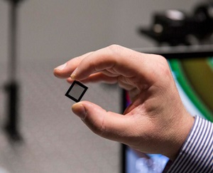
A promising route to smaller, powerful cameras built into smartphones and other devices is to design optical elements that manipulate light by diffraction-the bending of light around obstacles or through small gaps-instead of refraction.
Wolfgang Heidrich and co-workers at KAUST's Visual Computing Center and the University of British Columbia (UBC) in Canada are at the forefront of developing new diffractive optical elements (DOEs) that can be printed on to small, thin substrates. The team combines their carefully-designed DOEs with advanced computational techniques that can greatly enhance the images produced by such small optical devices.
Heidrich came to KAUST in 2014 from UBC, where he previously developed very high contrast displays for television sets.
"We developed the first consumer-ready display technology that had a major computational component, in the sense that the hardware itself was not useful without substantial computation," he says. "The target image would be sent to the device, and then the device would have to perform some fairly sophisticated algorithms on the image (in real time!) to produce the best image contrast. It really instilled in me the need for hardware-software co-design, where you develop optics, electronics and algorithms at the same time so that they fit together in the best possible way."
More recently, Heidrich and co-workers have applied the same approach to computational imaging for cameras. One major problem they are addressing, called chromatic aberration, will be familiar to anyone who has played with triangular prisms to produce a rainbow - different wavelengths change direction by varying amounts when they are refracted by lenses, resulting in incorrect color distributions in images.
Chromatic aberration is an even greater problem when light is manipulated by diffraction, so DOEs suffer a loss of color fidelity and blurring that depends on the color distribution of the incoming light. To combat this, Heidrich and his co-workers designed a thin, light-weight DOE called a diffractive achromat to balance the focusing contributions of different wavelengths. Their results from testing this innovative new component were published in ACM Transactions on Graphics ("The diffractive acromat: full spectrum computational imaging with diffractive optics") , the top journal destination for computer graphics studies.
"In a regular DOE lens, the focus will be near-perfect for a single design wavelength, and progressively blurred as you move away from that design wavelength," explains Heidrich. "The diffractive achromat sacrifices a little bit of sharpness for the design wavelength in exchange for more sharpness at all other wavelengths. Any remaining blur can then be removed computationally."
The researchers applied the same combination of cutting-edge optics with computer algorithms in a recent study published in Scientific Reports ("Encoded diffractive optics for full spectrum computational imaging") that could lead to extremely small zoom lenses. They used computational algorithms to design two DOEs with particular shapes, such that when they are placed on top of each other, they represent a diffractive lens with a specific focal length.
Then comes the cleverest bit.
"As you rotate the two DOEs relative to each other, the focal length, or any other parameter of the optical system, can change smoothly," says Heidrich. "One obvious application is to produce zoom lenses that do not require the lens barrel to move in and out of the camera for zooming."
Heidrich believes the active research environment at KAUST has been invaluable for pursuing his recent goals. "I have been able to assemble an interdisciplinary team, for more ambitious projects that take our hardware-software co-design to the next level," he says. "What's more, all our diffractive optical elements were built in the KAUST Nanofabrication Core Lab, which allowed quick turn-around times for experiments."
Computational imaging is still in its infancy, and provides many avenues that Heidrich and his co-workers hope to explore in coming years. Perhaps most excitingly, because DOEs are so thin, they don't absorb much energy from light as it passes through. This means that DOEs could, in principle, be used to manipulate any part of the electromagnetic spectrum, from radio waves to gamma rays.
Share on:


Suggested Items
iNEMI Packaging Tech Topic Series: Role of EDA in Advanced Semiconductor Packaging
04/26/2024 | iNEMIAdvanced semiconductor packaging with heterogenous integration has made on-package integration of multiple chips a crucial part of finding alternatives to transistor scaling. Historically, EDA tools for front-end and back-end design have evolved separately; however, design complexity and the increased number of die-to-die or die-to-substrate interconnections has led to the need for EDA tools that can support integration of overall design planning, implementation, and system analysis in a single cockpit.
Cadence, TSMC Collaborate on Wide-Ranging Innovations to Transform System and Semiconductor Design
04/25/2024 | Cadence Design SystemsCadence Design Systems, Inc. and TSMC have extended their longstanding collaboration by announcing a broad range of innovative technology advancements to accelerate design, including developments ranging from 3D-IC and advanced process nodes to design IP and photonics.
Ansys, TSMC Enable a Multiphysics Platform for Optics and Photonics, Addressing Needs of AI, HPC Silicon Systems
04/25/2024 | PRNewswireAnsys announced a collaboration with TSMC on multiphysics software for TSMC's Compact Universal Photonic Engines (COUPE). COUPE is a cutting-edge Silicon Photonics (SiPh) integration system and Co-Packaged Optics platform that mitigates coupling loss while significantly accelerating chip-to-chip and machine-to-machine communication.
Siemens’ Breakthrough Veloce CS Transforms Emulation and Prototyping with Three Novel Products
04/24/2024 | Siemens Digital Industries SoftwareSiemens Digital Industries Software launched the Veloce™ CS hardware-assisted verification and validation system. In a first for the EDA (Electronic Design Automation) industry, Veloce CS incorporates hardware emulation, enterprise prototyping and software prototyping and is built on two highly advanced integrated circuits (ICs) – Siemens’ new, purpose-built Crystal accelerator chip for emulation and the AMD Versal™ Premium VP1902 FPGA adaptive SoC (System-on-a-chip) for enterprise and software prototyping.
Listen Up! The Intricacies of PCB Drilling Detailed in New Podcast Episode
04/25/2024 | I-Connect007In episode 5 of the podcast series, On the Line With: Designing for Reality, Nolan Johnson and Matt Stevenson continue down the manufacturing process, this time focusing on the post-lamination drilling process for PCBs. Matt and Nolan delve into the intricacies of the PCB drilling process, highlighting the importance of hole quality, drill parameters, and design optimization to ensure smooth manufacturing. The conversation covers topics such as drill bit sizes, aspect ratios, vias, challenges in drilling, and ways to enhance efficiency in the drilling department.