


 Marcy's Musings: The Growing Industry
 It’s Only Common Sense: Here’s What To Do After IPC APEX EXPO 2024
 Dan’s Biz Bookshelf: Seeing the How
Nanotechnology Enables Powerful and Portable Sterilization Equipment
November 16, 2016 | Ohio State UniversityEstimated reading time: 2 minutes
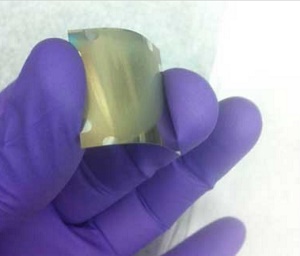
Engineers at The Ohio State University are developing the foil based LEDs for portable ultraviolet (UV) lights that can be used to purify drinking water and sterilize medical equipment.
In the journal Applied Physics Letters, the researchers describe how they designed the LEDs to shine in the high-energy "deep" end of the UV spectrum. The university will license the technology to industry for further development.
Deep UV light is already used by the military, humanitarian organizations and industry for applications ranging from detection of biological agents to curing plastics, explained Roberto Myers, associate professor of materials science and engineering at Ohio State.
The problem is that conventional deep-UV lamps are too heavy to easily carry around.
"Right now, if you want to make deep ultraviolet light, you've got to use mercury lamps," said Myers, who is also an associate professor of electrical and computer engineering. "Mercury is toxic and the lamps are bulky and electrically inefficient. LEDs, on the other hand, are really efficient, so if we could make UV LEDs that are safe and portable and cheap, we could make safe drinking water wherever we need it."
He noted that other research groups have fabricated deep-UV LEDs at the laboratory scale, but only by using extremely pure, rigid single-crystal semiconductors as substrates--a strategy that imposes an enormous cost barrier for industry.
Foil-based nanotechnology could enable large-scale production of a lighter, cheaper and more environmentally friendly deep-UV LED. But Myers and materials science doctoral student Brelon J. May hope that their technology will do something more: turn a niche research field known as nanophotonics into a viable industry.
"People always said that nanophotonics will never be commercially important, because you can't scale them up. Well, now we can. We can make a sheet of them if we want," Myers said. "That means we can consider nanophotonics for large-scale manufacturing."
In part, this new development relies on a well-established semiconductor growth technique known as molecular beam epitaxy, in which vaporized elemental materials settle on a surface and self-organize into layers or nanostructures. The Ohio State researchers used this technique to grow a carpet of tightly packed aluminum gallium nitride wires on pieces of metal foil such as titanium and tantalum.
The individual wires measure about 200 nanometers tall and about 20-50 nanometers in diameter--thousands of times narrower than a human hair and invisible to the naked eye.
In laboratory tests, the nanowires grown on metal foils lit up nearly as brightly as those manufactured on the more expensive and less flexible single-crystal silicon.
The researchers are working to make the nanowire LEDs even brighter, and will next try to grow the wires on foils made from more common metals, including steel and aluminum.
Share on:


Suggested Items
KIC’s Miles Moreau to Present Profiling Basics and Best Practices at SMTA Wisconsin Chapter PCBA Profile Workshop
01/25/2024 | KICKIC, a renowned pioneer in thermal process and temperature measurement solutions for electronics manufacturing, announces that Miles Moreau, General Manager, will be a featured speaker at the SMTA Wisconsin Chapter In-Person PCBA Profile Workshop.
The Drive Toward UHDI and Substrates
09/20/2023 | I-Connect007 Editorial TeamPanasonic’s Darren Hitchcock spoke with the I-Connect007 Editorial Team on the complexities of moving toward ultra HDI manufacturing. As we learn in this conversation, the number of shifting constraints relative to traditional PCB fabrication is quite large and can sometimes conflict with each other.
Standard Of Excellence: The Products of the Future
09/19/2023 | Anaya Vardya -- Column: Standard of ExcellenceIn my last column, I discussed cutting-edge innovations in printed circuit board technology, focusing on innovative trends in ultra HDI, embedded passives and components, green PCBs, and advanced substrate materials. This month, I’m following up with the products these new PCB technologies are destined for. Why do we need all these new technologies?
Experience ViTrox's State-of-the-Art Offerings at SMTA Guadalajara 2023 Presented by Sales Channel Partner—SMTo Engineering
09/18/2023 | ViTroxViTrox, which aims to be the world’s most trusted technology company, is excited to announce that our trusted Sales Channel Partner (SCP) in Mexico, SMTo Engineering, S.A. de C.V., will be participating in SMTA Guadalajara Expo & Tech Forum. They will be exhibiting in Booth #911 from the 25th to the 26th of October 2023, at the Expo Guadalajara in Jalisco, Mexico.
Intel Unveils Industry-Leading Glass Substrates to Meet Demand for More Powerful Compute
09/18/2023 | IntelIntel announced one of the industry’s first glass substrates for next-generation advanced packaging, planned for the latter part of this decade.