


 The Right Approach: I Hear the Train A Comin'
 It’s Only Common Sense: OCCAM—the Time Is Now
 Marcy's Musings: The Growing Industry
Terahertz Technology Has the Potential to Enable New Applications
November 28, 2016 | DEUTSCHES ELEKTRONEN-SYNCHROTRON DESYEstimated reading time: 4 minutes
In a multi-national effort, an interdisciplinary team of researchers from DESY and the Massachusetts Institute of Technology (MIT) has built a new kind of electron gun that is just about the size of a matchbox. Electron guns are used in science to generate high-quality beams of electrons for the investigation of various materials, from biomolecules to superconductors. They are also the electron source for linear particle accelerators driving X-ray free-electron lasers. The team of DESY scientist Franz Kärtner, who is also a professor at University of Hamburg and continues to run a research group at MIT, where he taught till 2010 before coming to Hamburg, presents its new electron gun in the scientific journal Optica.
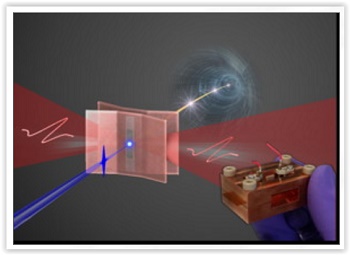
A miniature electron gun driven by Terahertz radiation: An ultraviolett pulse (blue) back-illuminates the gun photocathode, producing a high density electron bunch inside the gun. The bunch is immediately accelerated by ultra-intense single cycle Terahertz pulses to energies approaching one kilo-electronvolt (keV). These high-field optically-driven electron guns can be utilized for ultrafast electron diffraction or injected into the accelerators for X-ray light sources. Credit: W. Ronny Huang, CFEL/DESY/MIT
The new device uses laser generated terahertz radiation instead of the usual radio-frequency fields to accelerate electrons from rest. As the wavelength of the terahertz radiation is much shorter than radio-frequency radiation, the device can shrink substantially. While state-of-the-art electron guns can have the size of a car, the new device measures just 34 by 24.5 by 16.8 millimetres.
"Electron guns driven by terahertz radiation are miniature and efficient," explains main author Dr. W. Ronny Huang from MIT, who carried out this work at the Center for Free-Electron Laser Science CFEL in Hamburg, a cooperation of DESY, the University of Hamburg and the German Max Planck Society. "Also, the materials used to guide the radiation are susceptible to much higher fields at terahertz wavelengths as compared to radio frequency wavelengths, allowing terahertz radiation to give a much stronger 'kick' to the electrons. This has the effect of making the electron beams much brighter and shorter." Ultrashort electron beams with narrow energy spread, high charge and low jitter are essential for ultrafast electron diffraction experiments to resolve phase transitions in metals, semiconductors and molecular crystals, for example.
"Our device has a nanometer thin film of copper which, when illuminated with ultraviolett light from the back, produces short bursts of electrons," describes Huang. "Laser radiation with Terahertz frequency is fed into the device which has a microstructure specifically tailored to channel the radiation to maximize its impact on the electrons." This way the device reached an accelerating power of 350 Megavolts per metre. "The accelerating field was almost twice that of current state-of-the-art guns," says Huang. "We achieved an acceleration of a dense packet of 250,000 electrons from rest to 0.5 kilo-elecronvolts (keV) with minimal energy spread. Because of this, the electron beams coming out of the device could already be used for low-energy electron diffraction experiments."
In their set-up, the researchers used the large CFEL laser lab. The ultraviolet flash used to eject the electrons from the copper film is generated from the same laser as the accelerating terahertz radiation. "This ensures absolute timing synchronisation, substantially reducing jitter," explains Huang. The device worked stably over at least one billion shots, easing every-day operation.
"Electron guns are used ubiquitously for making atomic-resolution movies of chemical reactions via ultrafast electron diffraction as pioneered in Prof. Dwayne Miller's group at the Max Planck Institute for the Structure and Dynamics of Matter and CFEL," says Kärtner. "With smaller and better electron guns, biologists can gain better insight to the intricate workings of macromolecular machines, including those responsible for photosynthesis. And physicists can better understand the fundamental interaction processes in complex materials."
"Furthermore, electron guns are an important component of X-ray light source facilities," explains Kärtner. Next generation terahertz electron guns producing ultrashort and ultrabright electron bunches up to relativistic energies and of ten femtoseconds (quadrillionth of a second) duration are currently in development at CFEL, according to Kärtner. "These devices will be used as photo injectors for attosecond table-top free-electron lasers to be constructed within the program AXSIS," says Kärtner. An attosecond is a thousandth of a femtosecond. AXSIS (frontiers of Attosecond X-ray Science-Imaging and Spectroscopy) , funded by the European Research Council through an ERC Synergy Grant which also funded this work, also involves DESY scientists Prof. Henry Chapman and Dr. Ralph Aßman and Arizona State University Professor Petra Fromme.
About Deutsches Elektronen-Synchrotron DESY
Deutsches Elektronen-Synchrotron DESY is the leading German accelerator centre and one of the leading in the world. DESY is a member of the Helmholtz Association and receives its funding from the German Federal Ministry of Education and Research (BMBF) (90 per cent) and the German federal states of Hamburg and Brandenburg (10 per cent). At its locations in Hamburg and Zeuthen near Berlin, DESY develops, builds and operates large particle accelerators, and uses them to investigate the structure of matter. DESY's combination of photon science and particle physics is unique in Europe.
Share on:


Suggested Items
Designer’s Notebook: What Designers Need to Know About Manufacturing, Part 2
04/24/2024 | Vern Solberg -- Column: Designer's NotebookThe printed circuit board (PCB) is the primary base element for providing the interconnect platform for mounting and electrically joining electronic components. When assessing PCB design complexity, first consider the component area and board area ratio. If the surface area for the component interface is restricted, it may justify adopting multilayer or multilayer sequential buildup (SBU) PCB fabrication to enable a more efficient sub-surface circuit interconnect.
Insulectro’s 'Storekeepers' Extend Their Welcome to Technology Village at IPC APEX EXPO
04/03/2024 | InsulectroInsulectro, the largest distributor of materials for use in the manufacture of PCBs and printed electronics, welcomes attendees to its TECHNOLOGY VILLAGE during this year’s IPC APEX EXPO at the Anaheim Convention Center, April 9-11, 2024.
ENNOVI Introduces a New Flexible Circuit Production Process for Low Voltage Connectivity in EV Battery Cell Contacting Systems
04/03/2024 | PRNewswireENNOVI, a mobility electrification solutions partner, introduces a more advanced and sustainable way of producing flexible circuits for low voltage signals in electric vehicle (EV) battery cell contacting systems.
Heavy Copper PCBs: Bridging the Gap Between Design and Fabrication, Part 1
04/01/2024 | Yash Sutariya, Saturn Electronics ServicesThey call me Sparky. This is due to my talent for getting shocked by a variety of voltages and because I cannot seem to keep my hands out of power control cabinets. While I do not have the time to throw the knife switch to the off position, that doesn’t stop me from sticking screwdrivers into the fuse boxes. In all honesty, I’m lucky to be alive. Fortunately, I also have a talent for building high-voltage heavy copper circuit boards. Since this is where I spend most of my time, I can guide you through some potential design for manufacturability (DFM) hazards you may encounter with heavy copper design.
Trouble in Your Tank: Supporting IC Substrates and Advanced Packaging, Part 5
03/19/2024 | Michael Carano -- Column: Trouble in Your TankDirect metallization systems based on conductive graphite or carbon dispersion are quickly gaining acceptance worldwide. Indeed, the environmental and productivity gains one can achieve with these processes are outstanding. In today’s highly competitive and litigious environment, direct metallization reduces costs associated with compliance, waste treatment, and legal issues related to chemical exposure. What makes these processes leaders in the direct metallization space?