


 The Right Approach: I Hear the Train A Comin'
 It’s Only Common Sense: OCCAM—the Time Is Now
 Marcy's Musings: The Growing Industry
Electron Highway Inside Crystal
December 9, 2016 | University of WürzburgEstimated reading time: 4 minutes
Physicists at the University of Würzburg have made an astonishing discovery in a specific type of topological insulators. The effect is due to the structure of the materials used. The researchers have now published their work in the journal Science ("Robust spin-polarized midgap states at step edges of topological crystalline insulators").
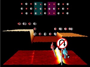
Step edges on topological crystalline insulators may lead to electrically conducting pathways where electrons with opposite spin spin move in converse directions -- any U-turn is prohibited. (Image: Thomas Bathon/Paolo Sessi/Matthias Bode)
Topological insulators are currently the hot topic in physics according to the newspaper Neue Zürcher Zeitung. Only a few weeks ago, their importance was highlighted again as the Royal Swedish Academy of Sciences in Stockholm awarded this year's Nobel Prize in Physics to three British scientists for their research of so-called topological phase transitions and topological phases of matter.
Topological insulators are also being studied at the Departments for Experimental Physics II and Theoretical Physics I of the University of Würzburg. However, they focus on a special version of insulators called topological crystalline insulators (TCI). In cooperation with the Polish Academy of Sciences in Warsaw and the University of Zurich, Würzburg physicists have now achieved a major breakthrough. They were able to detect new electronic states of matter in these insulators.
Step edges direct electrons
The central result: When crystalline materials are split, small atomically flat terraces emerge at the split off surfaces which are separated from each other by step edges. Inside these structures, conductive channels for electrical currents form which are extremely narrow at just about 10 nm and surprisingly robust against external disturbance. Electrons travel on these conductive channels with different spin in opposite directions - similar to a motorway with separate lanes for the two directions. This effect makes the materials interesting for technological applications in future electronic components such as ultra-fast and energy-efficient computers.
"TCIs are relatively simple to produce and they are already different from conventional materials because of their special crystalline structure," Dr. Paolo Sessi explains the background of the recently published paper. Sessi is a research fellow at the Department of Experimental Physics II and the lead author of the study.
Moreover, these materials owe their special quality to their electronic properties: In topological materials, the direction of spin determines the direction in which the electrons travel. Simply put, the "spin" can be interpreted as a magnetic dipole that can point in two directions ("up" and "down"). Accordingly, up-spin electrons in TCIs move in one and down-spin electrons in the other direction.
It's all about the number of atomic layers
"But previously scientists didn't know how to produce the conductive channels required to this end," says Professor Matthias Bode, Head of the Department for Experimental Physics II and co-author of the study. It was chance that now got the researchers on the right track: They discovered that very narrow conductive channels occur naturally when splitting lead tin selenide (PbSnSe), a crystalline insulator.
Step edges on the fragments' surfaces cause this phenomenon. They can be imaged using a high-resolution scanning tunnelling microscopy, or more precisely, the height of the corresponding step edges. "Edges that bridge an even number of atomic layers are totally inconspicuous. But if the edges span an odd number of atomic layers, a small area about 10 nm in width is created that has the electronic conductive channels properties we were looking for," Sessi explains.
Pattern breaks off at the edge
Supported by their colleagues from the Department of Theoretical Physics I and the University of Zurich, the experimental physicists were able to shed light on the origin of these new electronic states. To understand the principle, a little spatial sense is required:
"The crystalline structure causes a layout of the atoms where the different elements alternate like the black and white squares on a chessboard," Matthias Bode explains. This alternating black-and-white pattern applies to both squares which are adjacent and squares situated below and on top one another.
So if the crack of this crystal runs through different atomic layers, more than one edge is created there. Seen from above, white squares may also abut to other white squares along this edge and black squares to other black squares - or identical atoms to identical atoms. However, this only works if an odd number of atomic layers is responsible for the difference in height of the two surfaces.
Backed by calculations
"Calculations show that this offset at the surface is actually causative of these novel electronic states," says Paolo Sessi. Furthermore, they prove that the phenomenon of the spin-dependent conductive channels, which is characteristic of topological materials, occurs here as well.
According to the scientists, this property in particular makes the discovery relevant for potential applications, because such conductive channels cause low conduction loss on the one hand and can be used directly to transmit and process information in the field of spintronics on the other.
However, several questions need to be answered and challenges to be overcome before this will become reality. For instance, the scientists are not yet sure over which distances the currents in the newly discovered conductive channels can be transported. Also, in order to be implemented in circuits, methods would have to be developed that allow creating step edges of a defined height along specified directions.
Share on:


Suggested Items
SMC Korea 2024 to Highlight Semiconductor Materials Trends and Innovations on Industry’s Path to $1 Trillion
04/24/2024 | SEMIWith Korea a major consumer of semiconductor materials and advanced materials a key driver of innovation on the industry’s path to $1 trillion, industry leaders and experts will gather at SMC (Strategic Materials Conference) Korea 2024 on May 29 at the Suwon Convention Center in Gyeonggi-do, South Korea to provide insights into the latest materials developments and trends. Registration is open.
Groundbreaking Ceremony Marks the Beginning of a New Era for Newccess Industrial; The Construction of the MINGXIN Building
04/12/2024 | Newccess IndustrialOn a clear and sunny day in March, the groundbreaking ceremony for the MINGXIN Building took place in Shenzhen, China. This moment marked the official commencement of construction for a project that will reshape the semiconductor materials industry.
The Need for a Holistic Global Sustainability Standard
04/10/2024 | Michael Ford, Aegis SoftwareNo one can deny that the resources of our fragile planet are finite. The environment seems like a third party, subject to constant degradation. We’re acutely aware of the effects of pollution on our climate, and despite our “throw-away” culture, recycling and recovery of materials has remained relatively expensive, even as we use more energy just to survive.
iNEMI Publishes Four Roadmap Topics
04/04/2024 | iNEMIThe International Electronics Manufacturing Initiative (iNEMI) announces the availability of the first roadmap topics in the new iNEMI Roadmap format. Printed circuit boards, sustainable electronics, smart manufacturing, and mmWave materials and test are now available online.
Insulectro’s 'Storekeepers' Extend Their Welcome to Technology Village at IPC APEX EXPO
04/03/2024 | InsulectroInsulectro, the largest distributor of materials for use in the manufacture of PCBs and printed electronics, welcomes attendees to its TECHNOLOGY VILLAGE during this year’s IPC APEX EXPO at the Anaheim Convention Center, April 9-11, 2024.