


 The Right Approach: I Hear the Train A Comin'
 It’s Only Common Sense: OCCAM—the Time Is Now
 Marcy's Musings: The Growing Industry
A Bright (Nano) Light for Plasmonic Circuitry
January 13, 2017 | ICFOEstimated reading time: 2 minutes
The need of ever faster and powerful data processing and communication technologies, as well as for ultrasensitive and compact sensors is playing a crucial role in the advance of novel on-chip optical devices. It is a matter of time before integrated photonic circuits will become inherent in our daily lives in a similar way that electronic circuits did with the development of the transistor. Currently, one of the main goals in nano-photonics research is being able to integrate all the key necessary building blocks on a same chip, including the light source, transmission lines, modulators and detectors. Small on-chip lasers have emerged over the last decade as an ideal solution for the light source integration, however the main challenge is to efficiently couple their emission into the small footprint components.
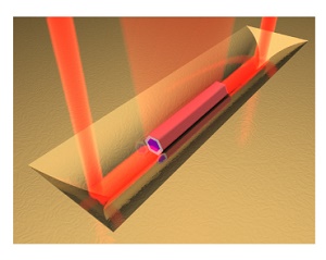
Now, in a recent Nanoletters publication, ICFO researcher Esteban Bermúdez-Ureña from the Plasmon Nano-optics group led by ICREA Prof. at ICFO Romain Quidant, in collaboration with the theory groups in Madrid led by Prof. Francisco J. García-Vidal and Prof. Jorge Bravo-Abad, the Laboratory for Semiconductor Materials at the EPFL in Switzerland led by Prof. Anna Fontcuberta i Morral, Dr. Cameron L.C. Smith from the TU Denmark, and Prof. Sergey I Bozhevolnyi at the Center for Nano Optics in Denmark, report on the realization of a novel ultra-compact hybrid nanolaser source operating at room temperature consisting of semiconductor nanowire (NW) lasers directly integrated with wafer-scale lithographically designed plasmonic waveguides.
To achieve this, the researchers used epitaxially grown GaAs NWs with diameters at least ten times smaller than a human hair and a few microns in length, which provided both the gain medium and the cavity geometry required for the lasing emission. The NWs were then transferred from their host substrate onto a silicon chip containing gold V-groove (VG) plasmonic waveguides, which support a special type of surface plasmons with sub-wavelength lateral electromagnetic field confinements and good propagation characteristics, namely the channel plasmon polaritons (CPPs). Later, by means of micro and nanomanipulation techniques, the researchers deterministically positioned individual NWs at the bottom of the VG channels, forming the so-called NW-VG hybrid nanolaser.
Lasing action and emission coupling to the CPP waveguide mode was observed upon pulsed illumination of the NW. Furthermore, rigorous theoretical simulations revealed that the lasing action in these devices was enabled by a hybrid photonic-plasmonic mode supported by the NW-VG geometry. The demonstrated system exhibited an unprecedented transfer efficiency of the lasing emission into the CPP waveguide mode of nearly 10%. This benchmark result was possible thanks to the good overlap between the hybrid plasmon lasing mode and the subwavelength confined CPP mode of the waveguide.
The authors envision that the unique features of the developed integrated source will provide the means to build high-sensitivity chemical or bio-sensing platforms powered by an integrated nanolaser. Future directions will also focus on the development of electrical injection as well as the integration of other on-chip components along the waveguide to build functional photonic circuitry.
Share on:


Suggested Items
Ansys, TSMC Enable a Multiphysics Platform for Optics and Photonics, Addressing Needs of AI, HPC Silicon Systems
04/25/2024 | PRNewswireAnsys announced a collaboration with TSMC on multiphysics software for TSMC's Compact Universal Photonic Engines (COUPE). COUPE is a cutting-edge Silicon Photonics (SiPh) integration system and Co-Packaged Optics platform that mitigates coupling loss while significantly accelerating chip-to-chip and machine-to-machine communication.
SEMI Applauds CHIPS Program Office Progress to Diversify U.S. Semiconductor Industry Workforce
04/18/2024 | SEMIThe SEMI Foundation, the arm of SEMI dedicated to supporting economic opportunity for workers and the sustained growth of the microelectronics industry by creating pathways and opportunities for job seekers, applauded strides made by the CHIPS Program Office to diversify the U.S. semiconductor industry workforce and its release of the First Annual Report Regarding the Opportunities and Inclusion Activities Undertaken by the Department of Commerce.
SEMI Applauds U.S. Chips Act Award for Samsung Electronics Facilities to Strengthen Domestic Semiconductor Supply Chain
04/17/2024 | SEMISEMI, the industry association serving the global electronics design and manufacturing supply chain, applauded the United States Department of Commerce’s announcement of a Preliminary Memorandum of Terms for an award under the CHIPS and Science Act to support the expansion of Samsung Electronics’ presence in Texas and the company’s development and production of leading-edge chips.
SIA Applauds CHIPS Act Incentives for Samsung Manufacturing Projects in Texas
04/16/2024 | SIAThe Semiconductor Industry Association (SIA) released the following statement from SIA President and CEO John Neuffer applauding semiconductor manufacturing incentives announced by the U.S. Department of Commerce and Samsung.
I-Connect007 Editor’s Choice: Five Must-Reads for the Week
04/12/2024 | Nolan Johnson, I-Connect007As we publish this week’s most-read news, the I-Connect007 team is wending its way home from an eventful and productive week at IPC APEX EXPO in Anaheim, California. We’ve posted a variety of dispatches from the show this week, released 73 realtimewith.com video interviews (and counting), and also gathered the content and updates you’ll be looking for in the upcoming issue of Show & Tell… IPC APEX EXPO 2024.