


 The Right Approach: I Hear the Train A Comin'
 It’s Only Common Sense: OCCAM—the Time Is Now
 Marcy's Musings: The Growing Industry
X-ray Imaging at Argonne Captures Material Defect Process
January 17, 2017 | Argonne National LaboratoryEstimated reading time: 3 minutes
From blacksmiths forging iron to artisans blowing glass, humans have for centuries been changing the properties of materials to build better tools – from iron horseshoes and swords to glass jars and medicine vials.
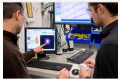
Argonne researchers are the first to capture the formation of nanomaterial defects in near-real time. Their work will help other researchers model the behavior of materials, a step that is key to engineering stronger, more reliable materials. (Image by Mark Lopez/Argonne National Laboratory.)
In modern life, new materials are created to improve today’s items, such as stronger steel for skyscrapers and more reliable semiconductors for cell phones.
Now, researchers at the Department of Energy’s (DOE) Argonne National Laboratory have discovered a new approach to detail the formation of these material changes at the atomic scale and in near-real time, an important step that could assist in engineering better and stronger new materials.
“What we’ve done is create a roadmap for other researchers. We’ve shown them a way to model this system and systems that have similar dynamics.”
In a study published Jan. 16 in Nature Materials, researchers at Argonne’s Advanced Photon Source, a DOE Office of Science User Facility, reveal they have captured – for the first time ever – images of the creation of structural defects in palladium when the metal is exposed to hydrogen.
This imaging capability will help researchers validate models that predict the behavior of materials and how they form defects. Defect engineering is the practice of intentionally creating defects within a material in order to change the material’s properties. This knowledge is key to engineering better, stronger and more reliable materials for buildings, semiconductors, batteries, technological devices and many other items and tools.
“Defect engineering is based on the idea that you can take something you already know the properties of and, by putting in defects or imperfections, engineer things with improved properties,” said Argonne scholar Andrew Ulvestad, one of the authors of the study. “The practice applies not only to metals but any material that has a crystal structure, like those found in solar cells and battery cathodes.”
Defect engineering is used to optimize material design across a variety of fields, but it is most commonly associated with the development of semiconductors. Semiconductor materials, like silicon, are used as electrical components; they form the foundation for most of our modern day electronics, including laptops and mobile phones.
In a process known as “doping,” manufacturers create defects in these materials by adding impurities in order to manipulate their electrical properties for various technological uses.
While manufacturers know they can change the properties of various materials to get the attributes they want, the processes that govern these changes are not always clear.
To increase the understanding of such processes, Argonne researchers focused specifically on defects forming on the nanoscale. Defects, interfaces and fluctuations at this very small level can provide critical insight into the functionalities of materials, such as their thermal, electronic and mechanical properties, on a larger scale.
To capture the formation of defects, the Argonne team took a nanostructured sample of palladium and injected, or infused, it with hydrogen at high-pressure. At the same time, they exposed the sample to powerful X-rays at the Advanced Photon Source.
Upon hitting the palladium crystal, the X-rays scattered, and their dispersion pattern was captured by a detector and used to calculate the changes in the position of atoms within the palladium structure. Essentially, this process enabled researchers to “see” deformations within the material.
“In some ways, we got the one-in-a-million shot, because defects occurring within the crystal don’t always happen due to the complex nature of the process,” said Argonne physicist Ross Harder, another author in the study.
The changes shown in the scans exemplify the numerous ways in which defects can alter the properties of materials and how they respond to external stimuli. For instance, the defects that formed altered the pressures at which palladium could store and release hydrogen, knowledge that could be useful for hydrogen storage, sensing and purification applications, the researchers said.
Defect engineering approaches are already being used to study other systems, including battery cathode nanoparticles. However, the study led by Ulvestad and Harder is the first to capture the formation of defects as they are happening.
“What we’ve done is create a roadmap for other researchers. We’ve shown them a way to model this system and systems that have similar dynamics,” Ulvestad said.
The study, titled “Three-dimensional imaging of dislocation dynamics during the hydriding phase transformation,” is published in Nature Materials. The work was funded by the DOE Office of Science and employed resources at the Advanced Photon Source, including beamlines 34-ID-C and 12-ID-D.
Share on:


Suggested Items
Real Time with... IPC APEX EXPO 2024: Sustainability in the Industry
04/26/2024 | Real Time with...IPC APEX EXPOGuest Editor Henry Crandall and Chris Nash of Indium Corporation discuss the company's 90th anniversary and its focus on sustainability. They focus on the benefits of sustainable materials, their compatibility, and value propositions. The conversation also highlights how Durafuse LT technology's role in reducing reflow temperatures is leading to significant cost and energy savings. Nash also touches on downstream sustainability efforts such as using recycled materials for packaging.
SMC Korea 2024 to Highlight Semiconductor Materials Trends and Innovations on Industry’s Path to $1 Trillion
04/24/2024 | SEMIWith Korea a major consumer of semiconductor materials and advanced materials a key driver of innovation on the industry’s path to $1 trillion, industry leaders and experts will gather at SMC (Strategic Materials Conference) Korea 2024 on May 29 at the Suwon Convention Center in Gyeonggi-do, South Korea to provide insights into the latest materials developments and trends. Registration is open.
Groundbreaking Ceremony Marks the Beginning of a New Era for Newccess Industrial; The Construction of the MINGXIN Building
04/12/2024 | Newccess IndustrialOn a clear and sunny day in March, the groundbreaking ceremony for the MINGXIN Building took place in Shenzhen, China. This moment marked the official commencement of construction for a project that will reshape the semiconductor materials industry.
The Need for a Holistic Global Sustainability Standard
04/10/2024 | Michael Ford, Aegis SoftwareNo one can deny that the resources of our fragile planet are finite. The environment seems like a third party, subject to constant degradation. We’re acutely aware of the effects of pollution on our climate, and despite our “throw-away” culture, recycling and recovery of materials has remained relatively expensive, even as we use more energy just to survive.
iNEMI Publishes Four Roadmap Topics
04/04/2024 | iNEMIThe International Electronics Manufacturing Initiative (iNEMI) announces the availability of the first roadmap topics in the new iNEMI Roadmap format. Printed circuit boards, sustainable electronics, smart manufacturing, and mmWave materials and test are now available online.