


 The Right Approach: I Hear the Train A Comin'
 It’s Only Common Sense: OCCAM—the Time Is Now
 Marcy's Musings: The Growing Industry
Researchers Produce Functional OLED Electrodes from Graphene
January 18, 2017 | Fraunhofer-GesellschaftEstimated reading time: 2 minutes
For the first time, it has been possible to produce functional OLED electrodes from graphene. The process was developed by Fraunhofer researchers together with partners from industry and research. The OLEDs can, for example, be integrated into touch displays, and the miracle material graphene promises many other applications for the future.
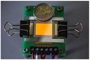
Orange luminous OLED on a graphene electrode. The two-euro coin serves as a comparison of sizes. (Image: Fraunhofer FEP)
The Fraunhofer Institute for Organic Electronics, Electron Beam and Plasma Technology FEP from Dresden, together with partners, has succeeded for the first time in producing OLED electrodes from graphene. The electrodes have an area of 2 × 1 square centimeters.
"This was a real breakthrough in research and integration of extremely demanding materials," says FEP’s project leader Dr. Beatrice Beyer.
The process was developed and optimized in the EU-funded project "Gladiator" (Graphene Layers: Production, Characterization and Integration) together with partners from industry and research.
Graphene is considered a new miracle material. The advantages of the carbon compound are impressive: graphene is light, transparent and extremely hard and has more tensile strength than steel. Moreover, it is flexible and extremely conductive for heat or electricity. Graphene consists of a single layer of carbon atoms which are assembled in a kind of honeycomb pattern. It is only 0.3 nanometers thick, which is about one hundred thousandth of a human hair. Graphene has a variety of applications – for example, as a touchscreen in smartphones.
Chemical reaction of copper, methane and hydrogen
The production of the OLED electrodes takes place in a vacuum. In a steel chamber, a wafer plate of high-purity copper is heated to about 800 degrees. The research team then supplies a mixture of methane and hydrogen and initiates a chemical reaction. The methane dissolves in the copper and forms carbon atoms, which spread on the surface. This process only takes a few minutes. After a cooling phase, a carrier polymer is placed on the graphene and the copper plate is etched away.
Gladiator project was launched in November 2013. The Fraunhofer team is working on the next steps until the conclusion in April 2017. During the remainder of the project, impurities and defects which occur during the transfer of the wafer-thin graphene to another carrier material are to be minimized. The project is supported by the EU Commission with a total of 12.4 million euros. The Fraunhofer Institute’s important industrial partners are the Spanish company Graphenea S.A., which is responsible for the production of the graphene electrodes, as well as the British Aixtron Ltd., which is responsible for the construction of the production CVD reactors.
Applications from photovoltaics to medicine
"The first products could already be launched in two to three years", says Beyer with confidence.
Due to their flexibility, the graphene electrodes are ideal for touch screens. They do not break when the device drops to the ground. Instead of glass, one would use a transparent polymer film. Many other applications are also conceivable: in windows, the transparent graphene could regulate the light transmission or serve as an electrode in polarization filters.
Graphene can also be used in photovoltaics, high-tech textiles and even in medicine.
Share on:


Suggested Items
Designer’s Notebook: What Designers Need to Know About Manufacturing, Part 2
04/24/2024 | Vern Solberg -- Column: Designer's NotebookThe printed circuit board (PCB) is the primary base element for providing the interconnect platform for mounting and electrically joining electronic components. When assessing PCB design complexity, first consider the component area and board area ratio. If the surface area for the component interface is restricted, it may justify adopting multilayer or multilayer sequential buildup (SBU) PCB fabrication to enable a more efficient sub-surface circuit interconnect.
Insulectro’s 'Storekeepers' Extend Their Welcome to Technology Village at IPC APEX EXPO
04/03/2024 | InsulectroInsulectro, the largest distributor of materials for use in the manufacture of PCBs and printed electronics, welcomes attendees to its TECHNOLOGY VILLAGE during this year’s IPC APEX EXPO at the Anaheim Convention Center, April 9-11, 2024.
ENNOVI Introduces a New Flexible Circuit Production Process for Low Voltage Connectivity in EV Battery Cell Contacting Systems
04/03/2024 | PRNewswireENNOVI, a mobility electrification solutions partner, introduces a more advanced and sustainable way of producing flexible circuits for low voltage signals in electric vehicle (EV) battery cell contacting systems.
Heavy Copper PCBs: Bridging the Gap Between Design and Fabrication, Part 1
04/01/2024 | Yash Sutariya, Saturn Electronics ServicesThey call me Sparky. This is due to my talent for getting shocked by a variety of voltages and because I cannot seem to keep my hands out of power control cabinets. While I do not have the time to throw the knife switch to the off position, that doesn’t stop me from sticking screwdrivers into the fuse boxes. In all honesty, I’m lucky to be alive. Fortunately, I also have a talent for building high-voltage heavy copper circuit boards. Since this is where I spend most of my time, I can guide you through some potential design for manufacturability (DFM) hazards you may encounter with heavy copper design.
Trouble in Your Tank: Supporting IC Substrates and Advanced Packaging, Part 5
03/19/2024 | Michael Carano -- Column: Trouble in Your TankDirect metallization systems based on conductive graphite or carbon dispersion are quickly gaining acceptance worldwide. Indeed, the environmental and productivity gains one can achieve with these processes are outstanding. In today’s highly competitive and litigious environment, direct metallization reduces costs associated with compliance, waste treatment, and legal issues related to chemical exposure. What makes these processes leaders in the direct metallization space?